

Polymeric conductive donor and transfer method
a polymer conductive donor and transfer method technology, applied in the field of donor laminates, can solve the problems of limiting the range of potential applications, low flexibility of such electrodes, and high cost of fabrication methods, and achieve the effects of accurate transfer of images, improved contrast in transferred images, and clean image edges
- Summary
- Abstract
- Description
- Claims
- Application Information
AI Technical Summary
Benefits of technology
Problems solved by technology
Method used
Image

Examples
examples
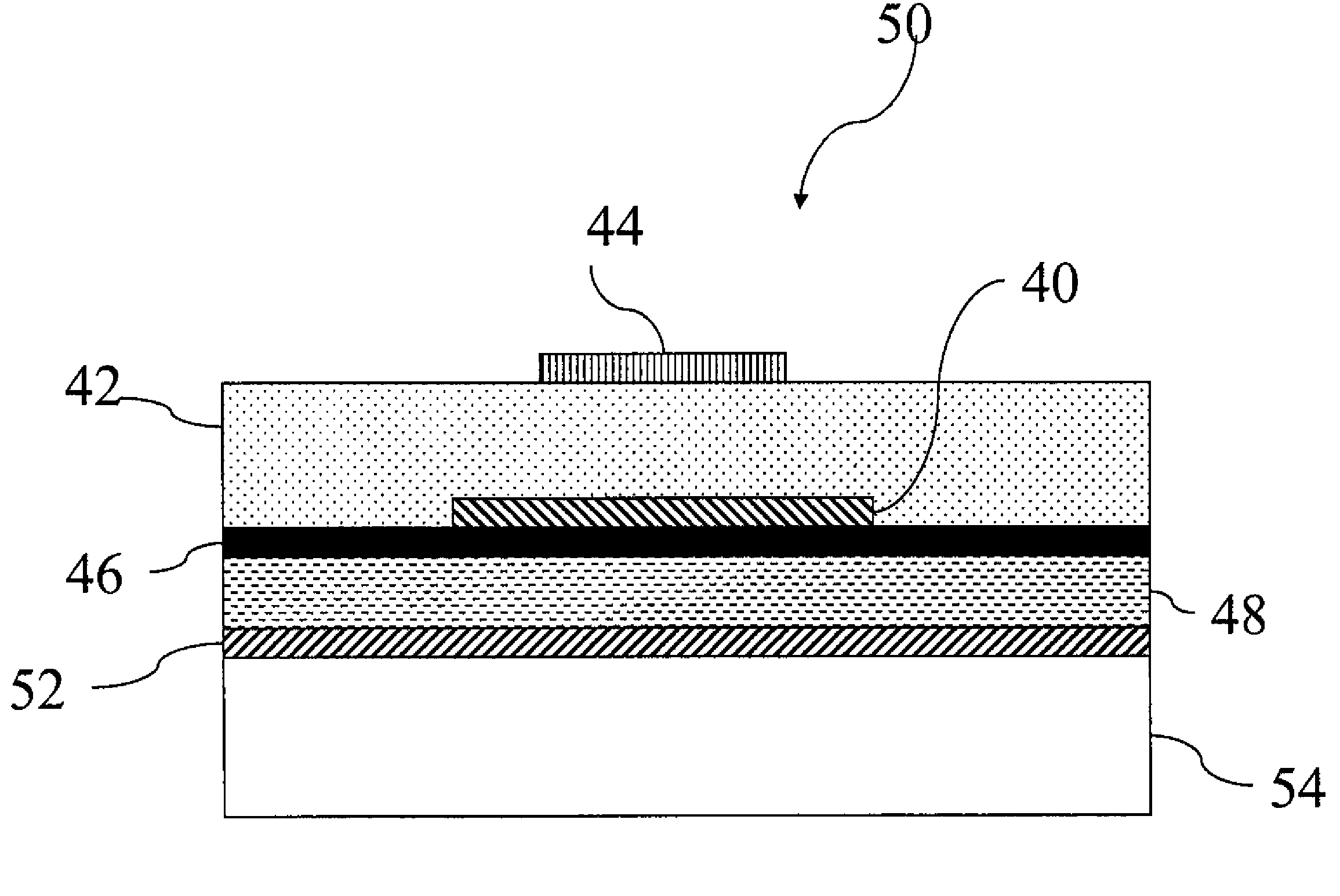
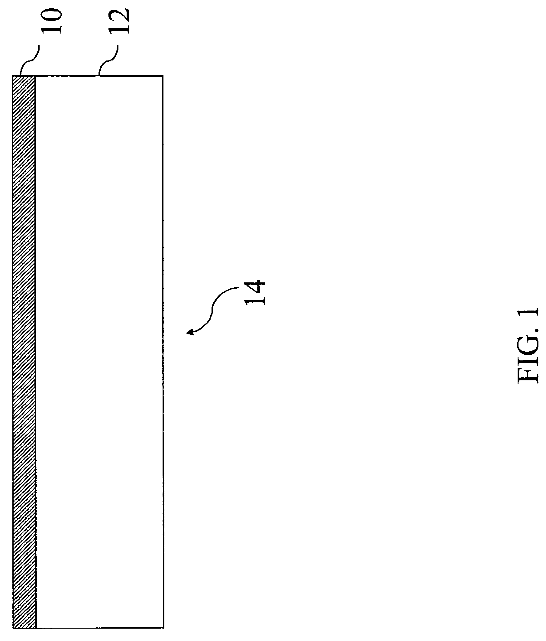
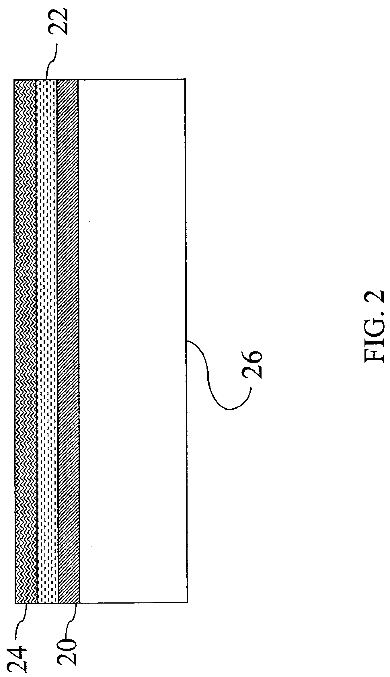
Donor Laminates
[0167]The following ingredients were used to form the coating composition for forming the donor laminate examples:
Ingredients for Coating Composition
[0168](a) Baytron P HC: aqueous dispersion of electronically conductive polythiophene and polyanion, namely, poly(3,4-ethylene dioxythiophene styrene sulfonate), supplied by H. C. Starck;
(b) Ludox AM: aqueous dispersion of alumina modified silica, supplied by Du Pont.
(c) Triton X 100: nonionic surfactant supplied by Dow Chemical Company;
(d) N-methylpyrrolidone: conductivity enhancing agent supplied by Acros;
(e) diethylene glycol: conductivity enhancing agent supplied by Aldrich;
(f) Silquest A 187: 3-glycidoxy-propyltrimethyoxysilane supplied by Crompton Corporation and
(g) isopropanol;
The following coating composition A was prepared for coating suitable substrates to form the laminate examples, as per invention:
Coating composition ABaytron ® P HC (1.3% aqueous)79.84 g Ludox AM8.87 gTriton ® X 100 (10% aqueous) 0.5 gN-methy...
PUM
| Property | Measurement | Unit |
|---|---|---|
| particle size | aaaaa | aaaaa |
| particle size | aaaaa | aaaaa |
| weight % | aaaaa | aaaaa |
Abstract
Description
Claims
Application Information