Method for manufacturing nano-array electrode and photoelectric conversion device using same

a technology of photoelectric conversion device and nano-array electrode, which is applied in the field of nano-array electrodes, can solve the problems of affecting the enhancement of productivity, the deactivation of the elementary excitation state of the electron, and the difficulty in accurately controlling the structure of the particle, etc., and achieves the effect of high performan

Inactive Publication Date: 2010-06-03
NIPPON OIL CORP
View PDF13 Cites 12 Cited by
  • Summary
  • Abstract
  • Description
  • Claims
  • Application Information

AI Technical Summary

Benefits of technology

[0004]For example, the most commonly used semiconductor material for dye-sensitized solar cells is titanium oxide (see, for example, Document 1 given below). The solar cells includes functional electrodes formed by forming a film of titanium oxide particles a few tens of nanometers in size on a transparent electrically conductive substrate and allowing a dye to adsorb thereon. It has been reported that the photo-conversion efficiency of this functional electrode depends largely on the structure of the titanium oxide layer such as the shape of titanium oxide particles and the bonding state thereof. The portions wherein titanium oxide particles bond to each other form barriers to the passage of photo-generated electrons through the titanium oxide layer to the transparent electrically conductive substrate. Due to the formation of the barriers, sufficient advantageous effects to enhance the solar energy conversion efficiency have not been able to be obtained even though the titanium oxide layer is thickened and a larger amount of dye is adsorbed thereto. In order to enhance the solar energy conversion efficiency, it has been attempted to control the structure of titanium oxide particles forming the titanium oxide layer (see, for example, Documents 2 to 8). However, it is difficult to accurately control the structure of particles, and at the same time an issue concerning the enhancement of the productivity also arises.
[0005]For enhancing the efficiency of an organic film type solar cell, it is necessary to establish a combination of an electron-donating organic semiconductor (donor) and an electron-accepting organic semiconductor (acceptor), a so-called heterojunction structure. An effective charge separation occurs in the proximity of the interface between the donor and the acceptor. Based on such an idea, Patent Documents 1 and 2 below proposed the use of a so-called bulk heterojunction wherein an electric conductive polymer as a donor and a fullerene derivative as an acceptor are mixed, thereby successfully developing a device with higher photoelectric converting efficiency than the conventional layered structure devices. In order to further enhance the efficiency, it is necessary to precisely control the interface structure between the donor and acceptor. However, there is a problem that it is difficult to control the structure by the mere mixing of the donor and acceptor.
[0008]Non-Patent Document 1: “NATURE” (Great Britain) 1991, VOL. 353, page 737 by B. O'Regan and M. Gratzel
[0009]Non-Patent Document 2: “Nano Letters” (U.S.A.) 2001, VOL. 1, page 637 by M. S. Won, Esther S. Jeng, and Jackie Y. Ying
[0010]Non-Patent Document 3: “Journal of American Chemical Society” (U.S.A.) 1998, VOL. 120, page 6832 by M. Ohtaki et al.
[0011]Non-Patent Document 4: “Advanced Materials” (U.S.A.) 2002, VOL. 14, page 309 by M. Yata, M. Mihara, S. Mouri, M. Kuroki, and T. Kijima

Problems solved by technology

When these electrons, phonons, or complexes thereof propagate through a semiconductor layer which is formed of aggregated semiconductor fine particles, scattering of the fine particles therein causes the deactivation of their elementary excitation state, which will be a problem when the performance of a functional device is intended to be improved.
However, it is difficult to accurately control the structure of particles, and at the same time an issue concerning the enhancement of the productivity also arises.
However, there is a problem that it is difficult to control the structure by the mere mixing of the donor and acceptor.Patent Document 1: U.S. Pat. No. 5,454,880Patent Document 2: U.S. Pat. No. 5,331,183Non-Patent Document 1: “NATURE” (Great Britain) 1991, VOL.

Method used


Image

  • Method for manufacturing nano-array electrode and photoelectric conversion device using same
  • Method for manufacturing nano-array electrode and photoelectric conversion device using same
  • Method for manufacturing nano-array electrode and photoelectric conversion device using same

Examples


example 1

[Manufacture of an Anodic-Oxide Porous Alumina Film]

[0196]An aluminum substrate (purity: 99.99%, manufactured by TOYO ALUMINIUM K.K.) was subjected to constant-current electrolysis at a temperature of 70° C. in a sulfuric acid-phosphoric acid mixed solution (85% 330 mL phosphoric acid, 75 mL concentrated sulfuric acid, 15 mL ethylene glycol, and 80 mL water) for 5 minutes by applying a current of 250 mA / cm2 to the aluminum substrate used as an anode and a black carbon used as a cathode and then washed with water and dried. An anodic oxidization was conducted at a temperature of 16° C. in an aqueous solution containing 0.5 mol / L oxalic acid for 5 hours by applying a voltage of 40 V to the aluminum substrate used as an anode and a black carbon used as a cathode. Thereafter, the aluminum substrate was dipped into a chromic acid-phosphoric acid mixed solution (6 g chromic oxide, 20 g phosphoric acid, and 300 g water) at a temperature of 50° C. for 12 hours and then washed with water and...

example 2

[Manufacture of an Anodic-Oxide Porous Alumina Film]

[0200]An aluminum substrate (purity: 99.99%, manufactured by TOYO ALUMINIUM K.K.) was subjected to constant-current electrolysis at a temperature of 70° C. in a sulfuric acid-phosphoric acid mixed solution (85% 330 mL phosphoric acid, 75 mL concentrated sulfuric acid, 15 mL ethylene glycol, and 80 mL water) for 5 minutes by applying a current of 250 mA / cm2 to the aluminum substrate used as an anode and a black carbon used as a cathode and then washed with water and dried. An anodic oxidization was conducted at a temperature of 16° C. in an aqueous solution containing 0.5 mol / L oxalic acid for 5 hours by applying a voltage of 40 V to the aluminum substrate used as an anode and a black carbon used as a cathode. Thereafter, the aluminum substrate was dipped into a chromic acid-phosphoric acid mixed solution (6 g chromic oxide, 20 g phosphoric acid, and 300 g water) at a temperature of 50° C. for 12 hours and then washed with water and...

example 3

[Manufacture of an Anodic-Oxide Porous Alumina Film]

[0204]An aluminum substrate (purity: 99.99%, manufactured by TOYO ALUMINIUM K.K.) was subjected to constant-current electrolysis at a temperature of 70° C. in a sulfuric acid-phosphoric acid mixed solution (85% 330 mL phosphoric acid, 75 mL concentrated sulfuric acid, 15 mL ethylene glycol, and 80 mL water) for 5 minutes by applying a current of 250 mA / cm2 to the aluminum substrate used as an anode and a black carbon used as a cathode and then washed with water and dried. An anodic oxidization was conducted at a temperature of 16° C. in an aqueous solution containing 0.3 mol / L sulfuric acid for 8 hours by applying a voltage of 25 V to the aluminum substrate used as an anode and a black carbon used as a cathode. Thereafter, the aluminum substrate was dipped into a chromic acid-phosphoric acid mixed solution (6 g chromic oxide, 20 g phosphoric acid, and 300 g water) at a temperature of 50° C. for 12 hours and then washed with water a...


PUM

PropertyMeasurementUnit
temperatureaaaaaaaaaa

Abstract

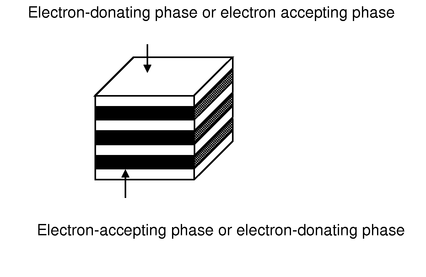
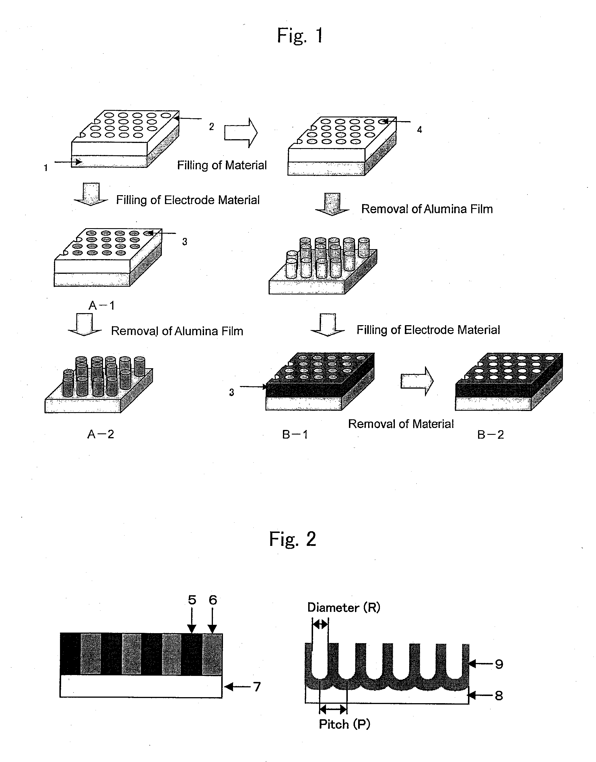
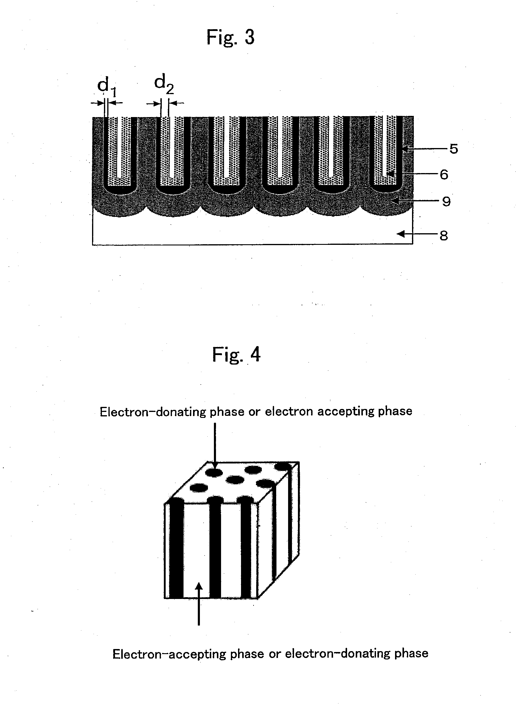
The present invention provides a method of manufacturing a nano-array electrode with a controlled nano-structure by filling a compound having an electron-accepting structure or an electron donating structure into the fine pores of an anodic-oxide porous alumina film obtained by anodically oxidizing aluminum in electrolyte. The spaces defined between the nano-arrays formed of the compound by removing the alumina film are filled with a compound having an electron-donating structure if the nano-arrays have an electron-accepting structure and a compound having an electron-accepting structure if the nano-arrays have an electron-donating structure. A high-performance, high-efficiency photoelectric converting device comprising a nano-array electrode manufactured by the method is also disclosed.

Description

CROSS-REFERENCE TO RELATED APPLICATIONS[0001]This application is a divisional of co-pending U.S. patent application Ser. No. 11 / 424,242, filed Jun. 15, 2006, w is a continuation of International Application No. PCT / JP2004 / 016471, filed Oct. 29, 2004, which was published in the Japanese language on Jul. 7, 2005, under International Publication No. WO 2005 / 061762 A1 and the disclosure of which is incorporated herein by reference.BACKGROUND OF THE INVENTION[0002]The present invention relates to novel nano-array electrodes with a controlled nano-structure and photoelectric conversion devices using the same.[0003]Conventional electrooptic devices and photoelectrochemical devices usually contain functional electrodes wherein a semiconductor is formed as a film on a substrate with an electrically conductive film. The semiconductor is responsive to external factors such as heat, light and temperature changes and produces electrons, phonons, or complexes thereof depending on the environment....

Claims


Application Information

Patent Timeline
Patent Type & Authority Applications(United States)
IPC IPC(8): H01L31/00H01L31/18H01L31/042B81C99/00H01L31/04C25D11/04C25D11/18H01L21/28H01L29/06H01L31/0352H01L51/00H01M14/00
CPCB82Y10/00C25D11/18H01L31/0352C25D11/045H01L51/0595Y02E10/542H01L31/03529Y02P70/50H10K10/701
Inventor ASANO, TSUYOSHIKUBO, TAKAYANISHIKITANI, YOSHINORI
Owner NIPPON OIL CORP
Why Eureka
Try Eureka