Nitride semiconductor component layer structure on a group iv substrate surface

a technology of nitride semiconductor components and substrate surfaces, which is applied in the direction of basic electric elements, electrical equipment, crystal growth processes, etc., can solve the problems of poor crystal quality, amorphous or polycrystalline, and unsuitable for optoelectronic components that comply with present-day standards

Inactive Publication Date: 2010-06-03
AZZURRO SEMICON
View PDF6 Cites 25 Cited by
  • Summary
  • Abstract
  • Description
  • Claims
  • Application Information

AI Technical Summary

Problems solved by technology

More recent developments also permit epitaxial growth on a silicon (100) substrate surface, but with poorer crystal quality.
Known non-epitaxial deposition processes, such as sputtering, result in amorphous or polycrystalline, at best textured layers which are not monocrystalline, and which are unsuitable for optoelectronic components complying with present-day standards.
The disadvantage of diamond and indeed of germanium as substrate materials is generally their significantly higher price in comparison to silicon, as well as a lower melting point below 1000° C. in the case of germanium.
Producing thin-film components, such as high-efficiency LEDs, FETs or MEMS on Si(100) is difficult to achieve on account of the poor crystal quality, and on Si(111) due to...

Method used


Image

  • Nitride semiconductor component layer structure on a group iv substrate surface
  • Nitride semiconductor component layer structure on a group iv substrate surface
  • Nitride semiconductor component layer structure on a group iv substrate surface

Examples


Embodiment Construction

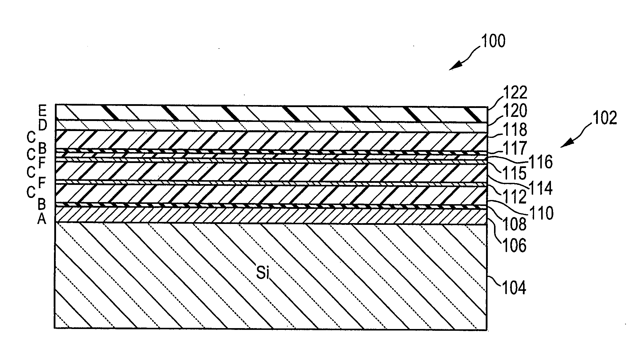
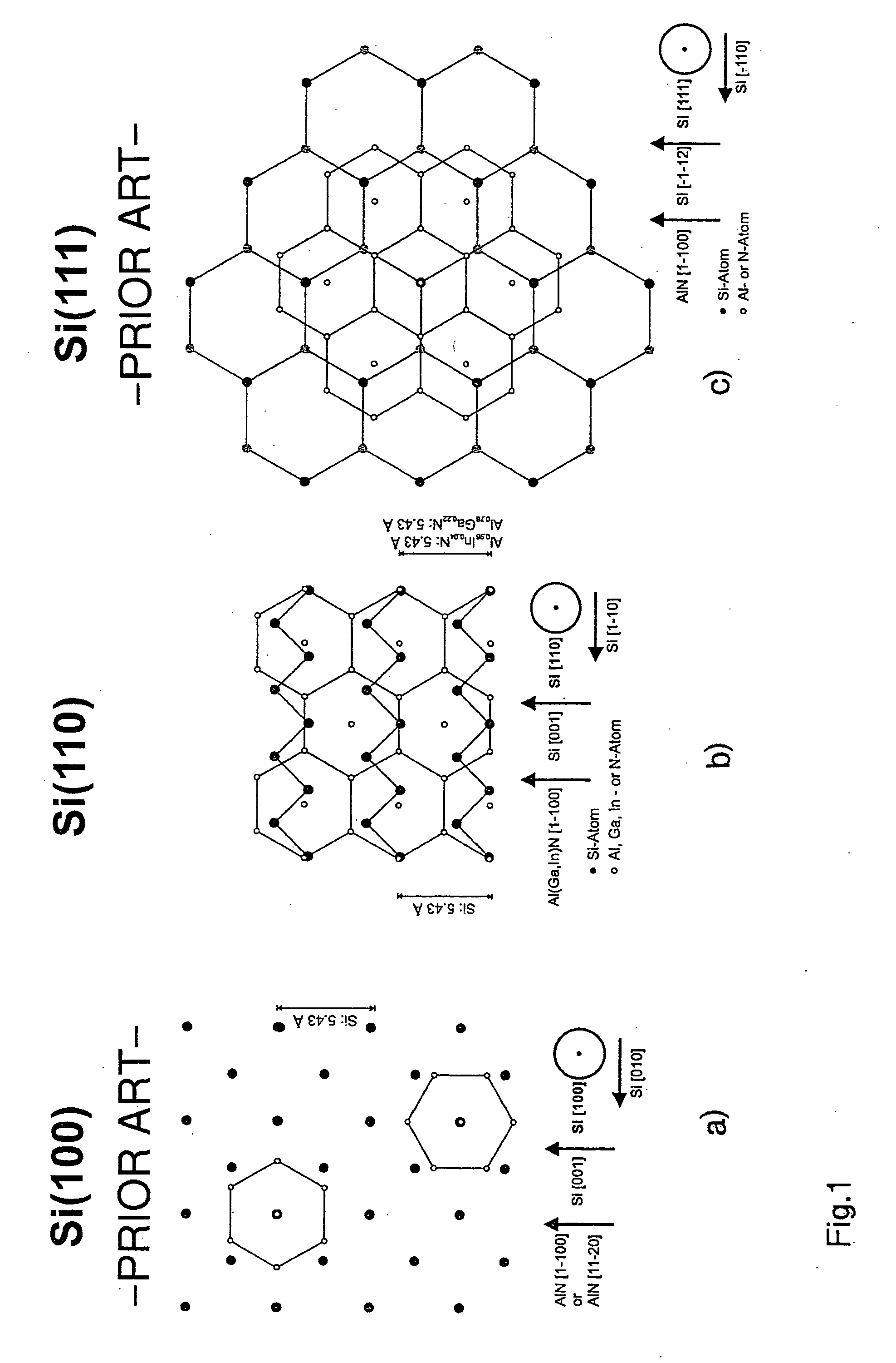
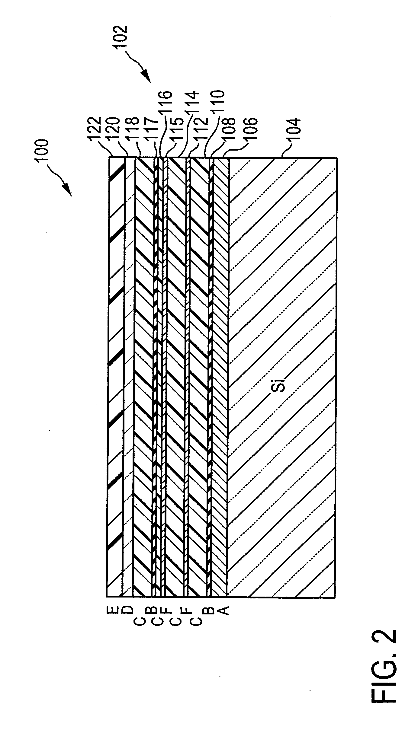
[0038]FIG. 1 shows, to explain one embodiment of a nitride semiconductor component and to compare this with solutions from the prior art, a plan view of a Group IV substrate surface in the form of a) a silicon (100), b) a silicon (110) and c) a silicon(111) surface, each having an Al1-x-yInxGayN covering, where 0≦x, yb) is relevant as an embodiment of the invention; the other two FIGS. 1a) and 1c) show, by way of comparison, the structure of substrate surfaces already used in the prior art. The best lattice matching in one direction is obtained when ternary materials are used for Al0.97In0.03N and Al0.78Ga0.22N. Even slight admixing of Ga and In is helpful in improving the material parameters. When a quaternary material is used, the ideal concentrations of In and Ga are correspondingly lower. However, higher concentrations are also possible and may be advantageous, depending on the process, since then the lattice mismatch in the [1-10] direction is also reduced, albeit at the cost o...


PUM


Abstract

The invention relates to nitride semiconductor component having a Group III nitride layer structure which is deposited on a substrate having a Group IV substrate surface made of a Group IV substrate material with a cubical crystal structure. The Group IV substrate surface has an elementary cell with C2 symmetry, but not with a higher rotational symmetry than C2 symmetry, when any surface reconstruction is ignored. The Group III nitride layer structure has a seeding layer of ternary or quaternary Al1-x-yInxGayN, where 0≦x, y<1 and x+y≦1, immediately adjacent to the Group IV substrate surface. High-quality monocrystalline growth is achieved as a result. The advantage of the invention consists in the high level of crystal quality that can be achieved, in the growth of c-, a- and m-plane GaN and above all in the ease with which the silicon substrate can be wholly or partially removed, since this is easier to do in a wet chemical process than on (111)-oriented substrates.

Description

CROSS REFERENCE TO RELATED APPLICATIONS[0001]This application is for entry into the U.S. national phase under §371 for International Application No. PCT / EP2008 / 055181 having an international filing date of Apr. 28, 2008, and from which priority is claimed under all applicable sections of Title 35 of the United States Code including, but not limited to, Sections 120, 363 and 365(c), and which in turn claims priority under 35 USC §119 to German Patent Application No. 10 2007 020 979.9 filed on Apr. 27, 2007, and U.S. Provisional Patent Application No. 60 / 926,444 filed on Apr. 27, 2007.BACKGROUND OF THE INVENTION[0002]1. Technical Field[0003]The present invention relates to a nitride semiconductor component having a Group III nitride layer structure on a Group IV substrate surface such as silicon, germanium, diamond or a mixed crystal within this system of Group IV semiconductors.[0004]2. Discussion of Related Art[0005]C-axis oriented gallium nitride GaN, grown epitaxially on a silicon...

Claims


Application Information

Patent Timeline
IPC IPC(8): H01L29/20H01L21/20
CPCH01L21/02433C30B29/403H01L21/02373H01L21/0254C30B25/02H01L21/02381H01L21/02609H01L33/007H01L21/02458H01L21/20
Inventor DADGAR, ARMINKROST, ALOIS
Owner AZZURRO SEMICON
Why Eureka
Try Eureka