Photomask blank manufacturing method and photomask manufacturing method

a manufacturing method and technology of photomask, applied in the field of photomask blank manufacturing methods, can solve the problems of affecting the performance of the mask, the degradation of the mask due to repeated use of the photomask, and the change of transmittance and phase difference, so as to achieve significant reduction of resolution and the effect of lowering the contrast at the pattern boundary

Active Publication Date: 2010-07-01
HOYA CORP
View PDF2 Cites 36 Cited by
  • Summary
  • Abstract
  • Description
  • Claims
  • Application Information

AI Technical Summary

Benefits of technology

[0012]It is therefore an object of this invention to provide photomask blank and photomask manufacturing methods that can improve the light fastness of a thin film such as a light-semitransmissive film to exposure light having a wavelength of 200 nm or less, thereby improving the lifetime of a photomask.
[0035]According to Aspect 1, by performing the treatment to modify (change the property of) the main surface of the thin film in advance, it is possible to suppress the oxidation rate of Si atoms forming the thin film and thus to suppress formation and enlargement of a modified layer conventionally caused by Si oxidation and expansion. Therefore, even if the photomask is repeatedly used with short-wavelength light, such as ArF excimer laser light, having a wavelength of 200 nm or less as exposure light so that the exposure light with the wavelength of 200 nm or less is accumulatively irradiated on the thin film pattern of the photomask, it is possible to suppress the change in transfer characteristic of the thin film pattern such as, for example, a change in transmittance, phase difference, or line width of a light-semitransmissive film.
[0037]The mechanism for the formation of the modified layer in the MoSi-based film, for example, is as described before and, in that case, the oxidation rate (dx / dt) of Si is given by dx / dt=k·C0 / N0, where k is an oxidation reaction coefficient on an oxidation interface, C0 is an O2 / H2O concentration on an oxidation interface, and N0 is the number of SiO2 molecules per unit volume. Therefore, for example, it is possible to suppress the oxidation rate of Si by increasing the value of NQ. Accordingly, by performing the treatment to modify the main surface of the thin film in advance to form the layer containing silicon and oxygen at the surface layer of the thin film as recited in Aspect 2, the number of SiO2 molecules at the surface layer of the thin film is increased to thereby suppress the oxidation rate of Si. By this, even if the photomask is irradiated with exposure light such as ArF excimer laser light in an environment containing H2O, O2, or O3, it is possible to effectively suppress formation and enlargement of a modified layer conventionally caused by Si oxidation and expansion. Therefore, even if the photomask is repeatedly used so that exposure light having a wavelength of 200 nm or less is accumulatively irradiated on the thin film pattern of the photomask, it is possible to suppress the change in transfer characteristic of the thin film pattern such as, for example, a change in transmittance, phase difference, or line width of a light-semitransmissive film.
[0040]According to Aspect 7, by forming a protective film on the formed thin film, it is possible to suppress the oxidation rate of Si atoms forming the thin film and thus to suppress formation and enlargement of a modified layer conventionally caused by Si oxidation and expansion. Therefore, even if the photomask is repeatedly used with short-wavelength light, such as ArF excimer laser light, having a wavelength of 200 nm or less as exposure light so that the exposure light with the wavelength of 200 nm or less is accumulatively irradiated on the thin film pattern of the photomask, it is possible to suppress the change in transfer characteristic of the thin film pattern such as, for example, a change in transmittance, phase difference, or line width of a light-semitransmissive film.
[0041]As recited in Aspect 8, the protective film is preferably made of a material containing silicon and oxygen. For example, by forming a protective film made of a material containing silicon and oxygen on a MoSi-based thin film to thereby increase the above-mentioned number of SiO2 molecules (No) at the surface of the thin film, it is possible to suppress the oxidation rate of Si.
[0044]By a photomask manufacturing method comprising a step of patterning the thin film in the photomask blank by etching as recited in Aspect 13, there is obtained a photomask improved in light fastness to short-wavelength exposure light such as ArF excimer laser light and thus significantly improved in mask lifetime.

Problems solved by technology

Following the reduction in exposure light wavelength in recent years, however, mask degradation due to repeated use of a photomask has become notable.
In the case of the phase shift mask, such changes in transmittance and phase difference are serious problems that affect the mask performance.
If the change in transmittance becomes large, the transfer accuracy is degraded, while if the change in phase difference becomes large, the phase shift effect at the pattern boundaries is difficult to obtain so that the contrast at the pattern boundaries is lowered and thus the resolution is significantly reduced.
Further, the change in line width degrades the CD accuracy of the photomask and finally degrades the CD accuracy of a pattern-transferred wafer.
Conventionally, for example, when haze is generated, cleaning is carried out for removing the haze, but a film loss (dissolution) due to the cleaning cannot be avoided and thus, roughly, the number of times of cleaning determines the mask lifetime.
However, since the number of times of cleaning is reduced due to an improvement to haze in recent years, the period of time of repeated use of a photomask is prolonged and thus the exposure time is prolonged correspondingly, and therefore, a problem of light fastness particularly to short-wavelength light such as ArF excimer laser light has been newly actualized.

Method used


Image

  • Photomask blank manufacturing method and photomask manufacturing method
  • Photomask blank manufacturing method and photomask manufacturing method

Examples


first embodiment

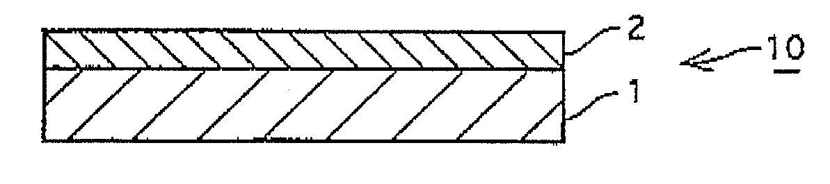
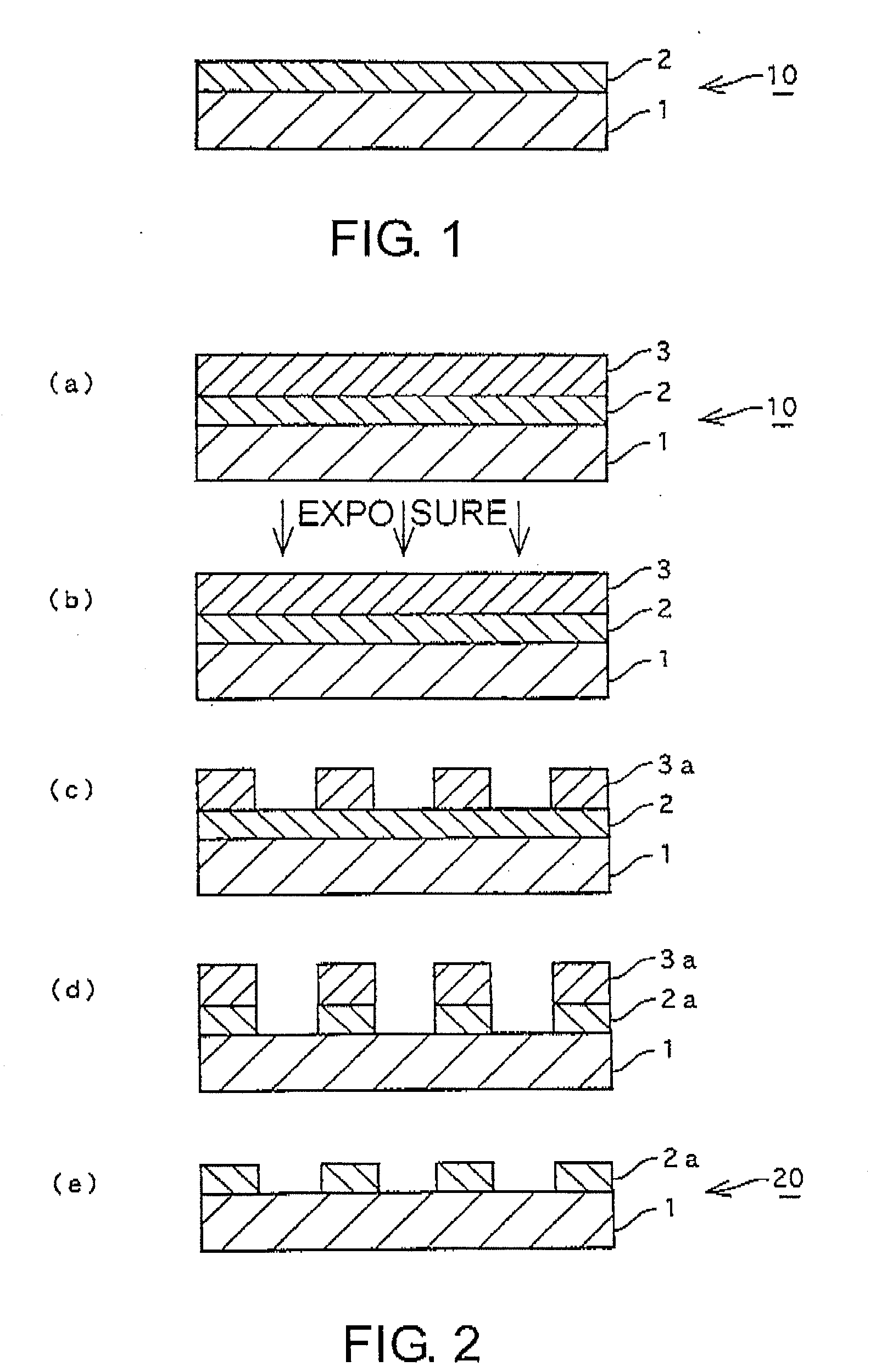
[0048]This embodiment is a method of manufacturing a photomask blank having, on a light-transmissive substrate, a thin film for forming a transfer pattern and comprises forming, on the light-transmissive substrate, the thin film made of a material containing a metal and silicon, and then performing a treatment to modify (change the property of) a main surface of the formed thin film in advance so that when exposure light having a wavelength of 200 nm or less is accumulatively irradiated on a thin film pattern of a photomask to be produced by patterning the thin film, the transfer characteristic of the thin film pattern does not change more than a predetermined degree.

[0049]The light-transmissive substrate is not particularly limited as long as it has transparency with respect to an exposure wavelength to be used. In this invention, a quartz substrate and various other glass substrates (e.g. soda-lime glass substrate, aluminosilicate glass substrate, etc.) can be used and, among them...

second embodiment

[0062]In this embodiment, as the treatment to modify the main surface of the thin film in advance, annealing by flash lamp irradiation is carried out in an atmosphere containing oxygen with an energy density of 5 to 14 J / cm2. If the irradiation energy density is less than 5 J / cm2, there is a problem that the wash resistance and the hot water resistance are reduced. On the other hand, if the irradiation energy density is higher than 14 J / cm2, there arises a possibility of degradation of the thin film itself.

[0063]In this invention, it is particularly preferable that the energy density in an atmosphere containing oxygen for the flash lamp annealing be in a range of 8 to 12 J / cm2.

[0064]In this embodiment, the flash lamp annealing is preferably carried out, for example, in the atmosphere or in an atmosphere containing oxygen and is particularly preferably carried out in an atmosphere containing oxygen (e.g. a mixed gas atmosphere of oxygen and nitrogen).

[0065]It is preferable that the s...

third embodiment

[0071]In this embodiment, as the treatment to modify the main surface of the thin film in advance, art oxygen plasma treatment is carried out. Specifically, the oxygen plasma treatment is carried out, for example, by setting the inside of a chamber to an oxygen gas atmosphere and applying a predetermined RF ICP power and RF bias power to thereby convert an oxygen gas into a plasma and irradiating the oxygen plasma on the thin film placed in the chamber.

[0072]It is preferable that the substrate coated with the thin film be heated in the oxygen plasma treatment.

[0073]The treatment time by the oxygen plasma irradiation (irradiation time) may be determined by taking into account both the oxygen plasma treatment conditions and the thickness of a surface layer, to be modified by the treatment, of the thin film and is, in general, suitably about 1 to 10 minutes.

[0074]In this embodiment, the thickness of the surface layer, modified by the oxygen plasma treatment to modify the main surface o...


PUM

PropertyMeasurementUnit
wavelengthaaaaaaaaaa
thicknessaaaaaaaaaa
thicknessaaaaaaaaaa

Abstract

A thin film made of a material containing a metal and silicon is formed on a light-transmissive substrate. Then, a treatment is performed to modify a main surface of the thin film in advance so that when exposure light having a wavelength of 200 nm or less is accumulatively irradiated on a thin film pattern of a photomask to be produced by patterning the thin film, the transfer characteristic of the thin film pattern does not change more than a predetermined degree. This treatment is performed by carrying out, for example, a heat treatment in an atmosphere containing oxygen at 450° C. to 900° C.

Description

[0001]This application is based upon and claims the benefit of priority from Japanese Patent Application No. 2008-335663, filed on Dec. 29, 2008, the disclosure of which is incorporated herein in its entirety by reference.TECHNICAL FIELD[0002]This invention relates to methods of manufacturing a photomask blank and a photomask and, in particular, relates to a method of manufacturing a photomask blank for use in the manufacture of a photomask to be suitably used in an exposure apparatus using exposure light having a short wavelength of 200 nm or less and to a method of manufacturing such a photomask.BACKGROUND ART[0003]Generally, fine pattern formation is carried out by photolithography in the manufacture of a semiconductor device. A number of substrates called photomasks are normally used for such fine pattern formation. The photomask comprises generally a light-transmissive glass substrate having thereon a fine pattern made of a metal thin film or the like. The photolithography is u...

Claims


Application Information

Patent Timeline
Patent Type & Authority Applications(United States)
IPC IPC(8): G03F1/00G03F1/50G03F1/54
CPCG03F1/32G03F1/50H01L21/0332H01L21/0337
Inventor SUZUKI, TOSHIYUKIHASHIMOTO, MASAHIROONO, KAZUNORIOHKUBO, RYOSAKAI, KAZUYA
Owner HOYA CORP
Why Eureka
Try Eureka