

Organic photoelectric device and material used therein
a photoelectric device and organic technology, applied in the direction of organic semiconductor devices, thermoelectric devices, organic chemistry, etc., can solve the problems of deterioration of luminous efficiency, high manufacturing cost, and increased driving voltag
- Summary
- Abstract
- Description
- Claims
- Application Information
AI Technical Summary
Benefits of technology
Problems solved by technology
Method used
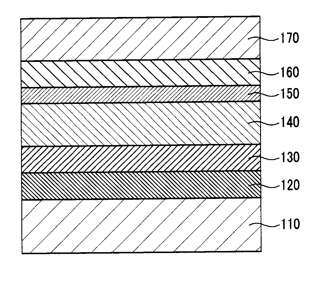
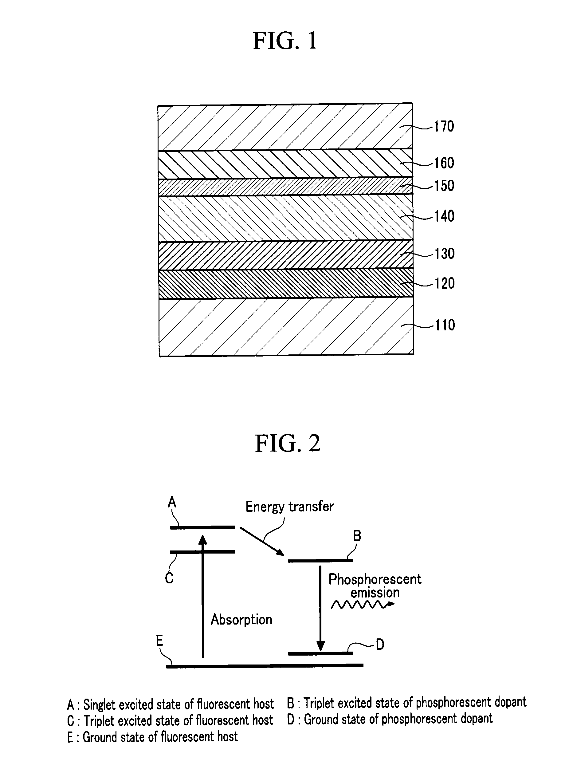
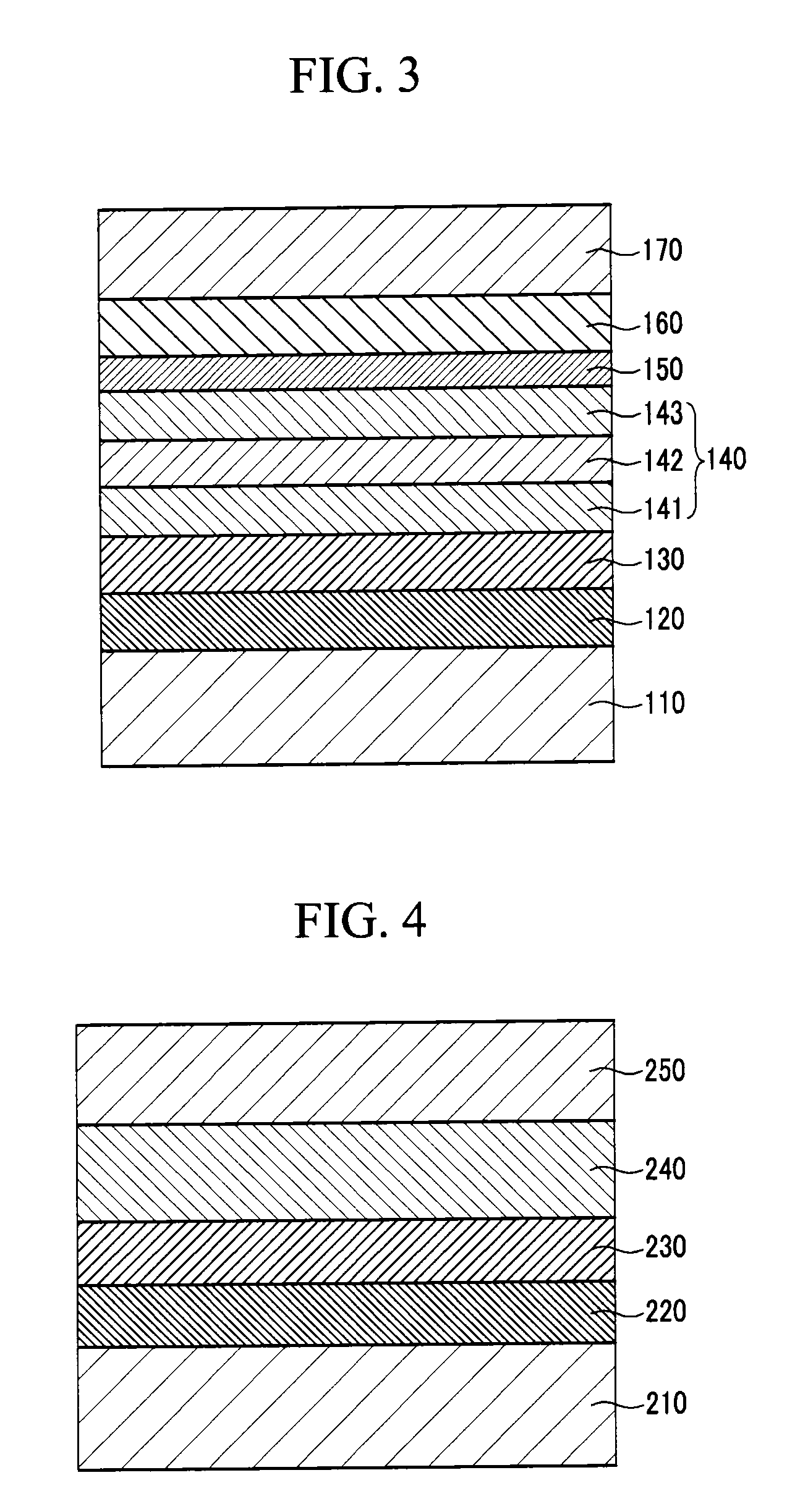
Image

Examples
example 1
[0127]A Corning 15 Ω / cm2 (1200 Å) ITO glass substrate was cut into a size of 50 mm×50 mm×0.7 mm, subjected to ultrasonic wave cleaning in each of isopropyl alcohol and pure water for 5 minutes, and subjected to the UV and ozone cleaning for 30 minutes.
[0128]N,N′-di(1-naphthyl)-N,N′-diphenylbenzidine (NPD) was evaporated on the surface of the substrate, to provide a hole transport layer (HTL) in a thickness of 40 nm.
[0129]On the surface of the hole transport layer (HTL), a host material (Bepp2) represented by the above Formula 40 and tris(2-phenylpyridine)iridium (Ir(ppy)3) dopant were deposited at the same time to provide an emission layer, and a LiF / Al cathode was deposited thereon to provide a green organic light emitting diode (OLED). The thickness and material used for each layer are described in the following Table 2.
example 2
[0136]A Corning 15 Ω / cm2 (1200 Å) ITO glass substrate was cut into a size of 50 mm×50 mm×0.7 mm, subjected to ultrasonic wave cleaning in each of isopropyl alcohol and pure water for 5 minutes, and subjected to UV and ozone cleaning for 30 minutes.
[0137]N,N′-di(1-naphthyl)-N,N′-diphenylbenzidine (NPD) was evaporated on the surface of substrate at a thickness of 40 nm to provide a hole transport layer (HTL).
[0138]A Bepq2 host material represented by the above Formula 37 and a tris(1-phenylisoquinoline)iridium (Ir(piq)3) dopant were deposited on the surface of hole transport layer (HTL) at the same time to provide an emission layer, and a LiF / Al cathode was deposited thereon to provide a red organic light emitting diode (OLED). The thickness and material used for each layer are shown in the following Table 4.
example 3
[0139]A Corning 15 Ω / cm2 (1200 Å) ITO glass substrate was cut into a size of 50 mm×50 mm×0.7 mm, subjected to ultrasonic wave cleaning in each of isopropyl alcohol and pure water for 5 minutes, and subjected to UV and ozone cleaning for 30 minutes.
[0140]N,N′-di(1-naphthyl)-N,N′-diphenylbenzidine (NPD) was evaporated on the surface of the substrate at a thickness of 40 nm to provide a hole transport layer (HTL).
[0141]A Bepq2 host material represented by the above Formula 37 and a tris(1-phenylisoquinoline)iridium (Ir(piq)3) dopant were deposited on the surface of the hole transport layer at the same time to provide an emission layer.
[0142]The compound represented by Chemical Formula 8 was evaporated on the surface of the emission layer at a thickness of 5 nm to provide an electron transport layer. On the electron transport layer, a LiF / Al cathode was deposited to provide a red organic light emitting diode. The thickness and material used for each layer are shown in the following Tabl...
PUM
 Abstract
Description
Claims
Application Information