Semiconducting nanowire arrays for photovoltaic applications

a technology of photovoltaic applications and nanowire arrays, which is applied in the direction of semiconductor devices, electrical devices, solid-state devices, etc., can solve the problems of high module cost and impede the market acceptance of this clean alternative approach, and achieve the effect of new design attributes and readily produced

Inactive Publication Date: 2010-08-05
ILLUMINEX CORP
View PDF55 Cites 62 Cited by
  • Summary
  • Abstract
  • Description
  • Claims
  • Application Information

AI Technical Summary

Benefits of technology

[0009]This process for the versatile production of SiNWs enables a new generation of solar electric devices that are lightweight, versatile, low-cost, and posses novel design attributes. Nano-PV electricity generation using readily produced, diverse implementations can be realized including: conformal fitting Al foils or applied Al layers for PV coatings on the bodies of electric cars, spools of SiNW-on-Al threads for PV textile applications, or simply Al deposited on glass panels or other insulating substrates to compete head-to-head with the established and dominant Si wafer-based PV device market.

Problems solved by technology

While efforts are on-going to push cell efficiencies closer to the theoretical limit of 31% for a single bandgap silicon solar conversion device, high module cost impedes market acceptance of this clean, alternative approach to electrical power generation, largely due to the production costs of the silicon wafers used to manufacture the photovoltaic modules.

Method used


Image

  • Semiconducting nanowire arrays for photovoltaic applications
  • Semiconducting nanowire arrays for photovoltaic applications
  • Semiconducting nanowire arrays for photovoltaic applications

Examples


Embodiment Construction

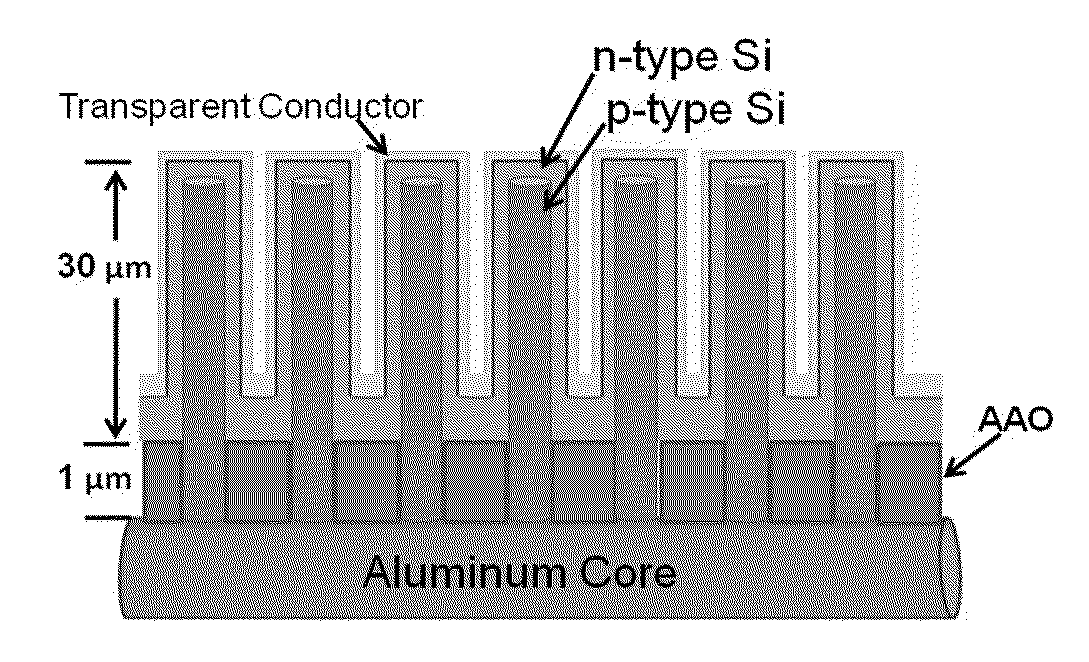
[0029]This invention relates to the growth and use of nanowires on substrates in order to produce electrical circuits, including photovoltaic devices.

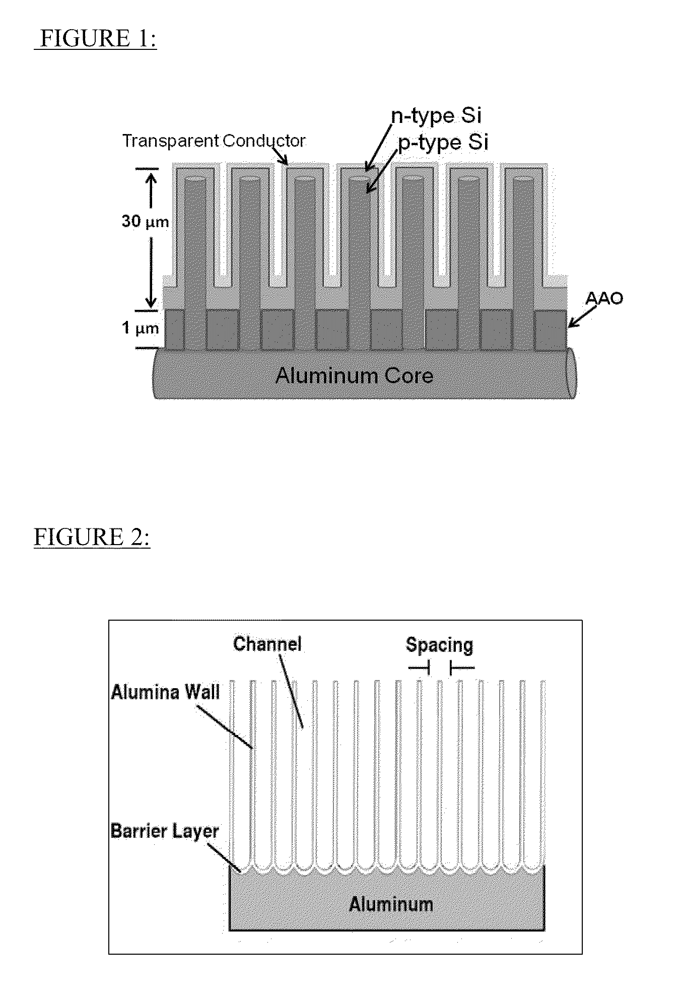
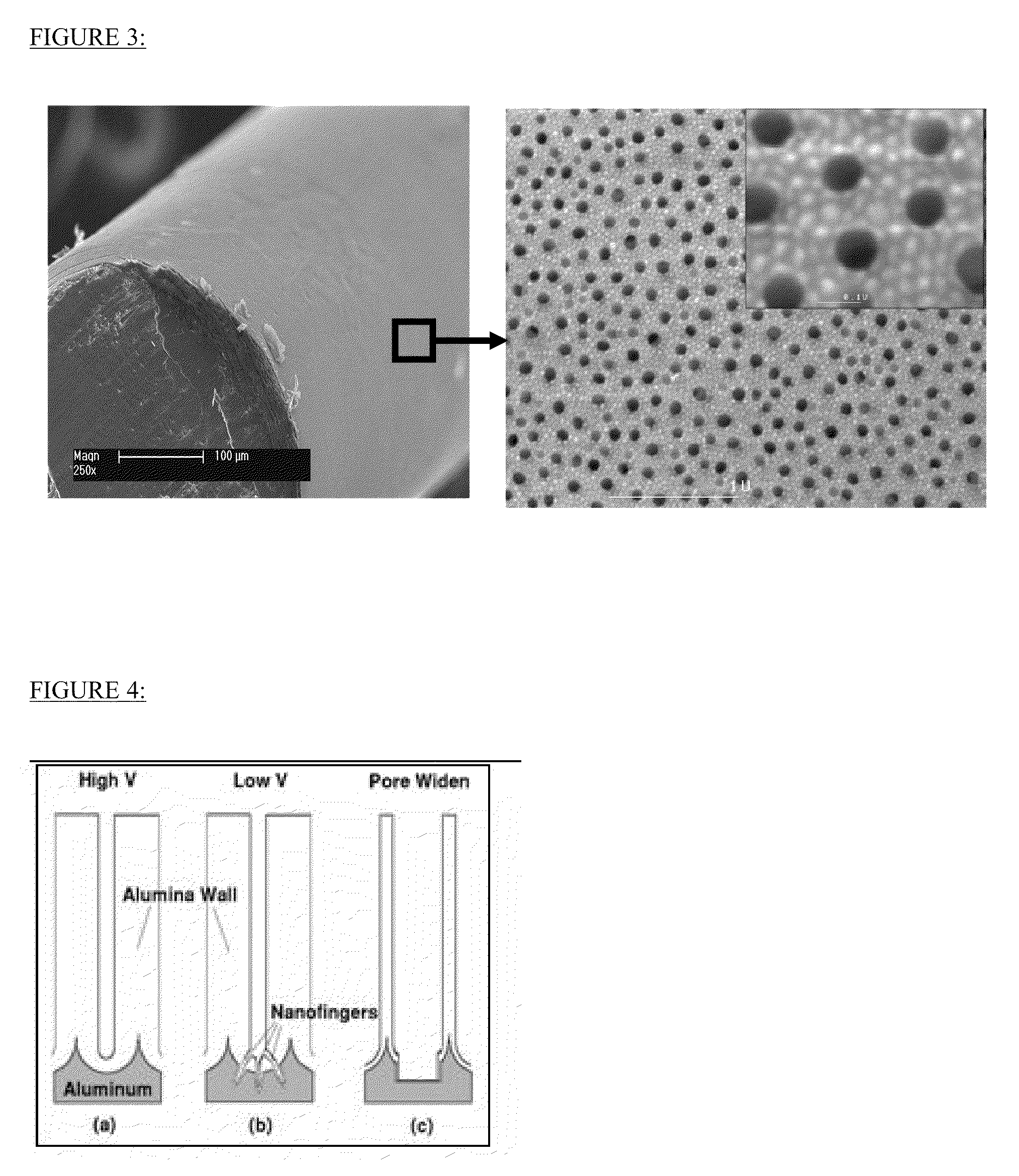
[0030]The present patent encompasses both the design of SiNW array based PV devices including components that comprise said PV devices, and, the basic process for the stepwise fabrication of silicon nanowire arrays (SiNWs) for PV or other device applications. The method for producing SiNW arrays on partially anodized Al or Al layers adhered to other material structures is presented, in addition to techniques for integrating the engineered SiNW arrays into PV device designs. Practitioners of ordinary skill in the art will readily recognize that the methods and designs described herein can be extended to starting materials other than Al, active opto-electronic nano-structures made from materials other than Si, and devices that utilize metallic and semiconducting nanoscale structures for fabrication and function other than photovoltaics. ...


PUM

PropertyMeasurementUnit
eutectic temperatureaaaaaaaaaa
temperaturesaaaaaaaaaa
length scaleaaaaaaaaaa

Abstract

This invention relates to the fabrication of nanowires for electrical and electronic applications. A method of growing silicon nanowires using an alumina template is disclosed whereby the aluminum forming the alumina is also used as the catalyst for growing the silicon nanowires in a VLS (CVD) process and as the semiconductor dopant. In addition, various techniques for masking off parts of the aluminum and alumina in order to maintain electrical isolation between device layers is disclosed.

Description

PRIORITY CLAIM[0001]This patent application hereby incorporates by reference and claims priority as a continuation in part to U.S. patent application Ser. Nos. 12 / 185,773 filed on Aug. 4, 2008, 11 / 917,505 filed on Dec. 14, 2007, the U.S. National Stage of PCT / US06 / 023662 filed on Jun. 16, 2006, with priority to 60 / 692,202 filed on Jun. 17, 2005 and as a continuation to U.S. Pat. App. Nos. 61 / 169,279 filed on Apr. 14, 2009, 61 / 177,265 filed on May 11, 2009 and 61 / 242,212 filed on Sep. 14, 2009, all of which are incorporated herein by reference.GOVERNMENT LICENSE RIGHTS[0002]The U.S. Government has a paid-up license in this invention and the right in limited circumstances to require the patent owner to license others on reasonable terms as provided for by the terms of Contract No. DOE-DE-FG02-07ER86313 awarded by The Department of Energy.SUMMARY OF THE INVENTION[0003]Single crystal or polycrystalline silicon solar cells are currently the dominant commercial photovoltaic (PV) technolog...

Claims


Application Information

Patent Timeline
Patent Type & Authority Applications(United States)
IPC IPC(8): H01L29/06H01L21/20
CPCH01L31/022466Y02E10/50H01L31/1884H01L31/03529
Inventor HABIB, YOUSSEF
Owner ILLUMINEX CORP
Why Eureka
Try Eureka