Method for manufacturing semiconductor device

a manufacturing method and semiconductor technology, applied in the direction of iron compounds, cobalt compounds, nickel compounds, etc., can solve the problems of not finding the manufacturing condition by which a semiconductor element using an oxide semiconductor can have favorable characteristics, and the characteristics of the oxide semiconductor itself have not been elucidated. to achieve the effect of favorable characteristics

Active Publication Date: 2010-09-16
SEMICON ENERGY LAB CO LTD
View PDF102 Cites 51 Cited by
  • Summary
  • Abstract
  • Description
  • Claims
  • Application Information

AI Technical Summary

Benefits of technology

[0017]In one embodiment of the disclosed invention, a first heat treatment is performed after a step of forming a semiconductor layer and before a step of forming an insulating layer which covers the semiconductor layer and the like; and a second heat treatment is performed after the step of forming the insulating layer which covers the semiconductor layer and the like. This makes it possible to provide a semiconductor device including a semiconductor element which has favorable characteristics.
[0018]The above-described effect is enhanced especially in such cases as the following: the case of using an oxide semiconductor layer containing indium, gallium, and zinc as the semiconductor layer; the case where a hydrogen concentration in the semiconductor layer is higher than a hydrogen concentration in the second insulating layer; the case where a nitrogen concentration in the semiconductor layer is higher than a nitrogen concentration in the second semiconductor layer; or the like.

Problems solved by technology

As seen from the above, an oxide semiconductor has been extensively researched; however, for its complex composition, the characteristics of the oxide semiconductor itself have not been elucidated.
The present situation is that under these circumstances, a manufacturing condition by which a semiconductor element using an oxide semiconductor can have favorable characteristics has not been found.

Method used


Image

  • Method for manufacturing semiconductor device
  • Method for manufacturing semiconductor device
  • Method for manufacturing semiconductor device

Examples


embodiment 1

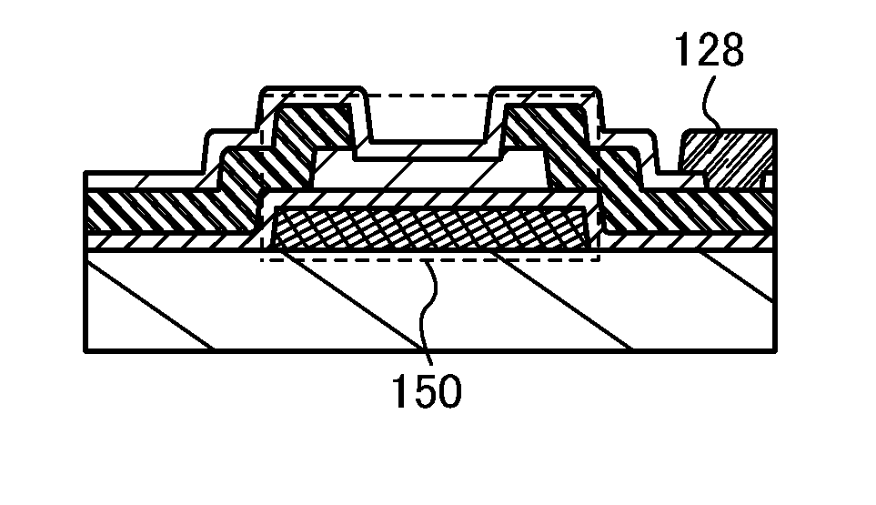
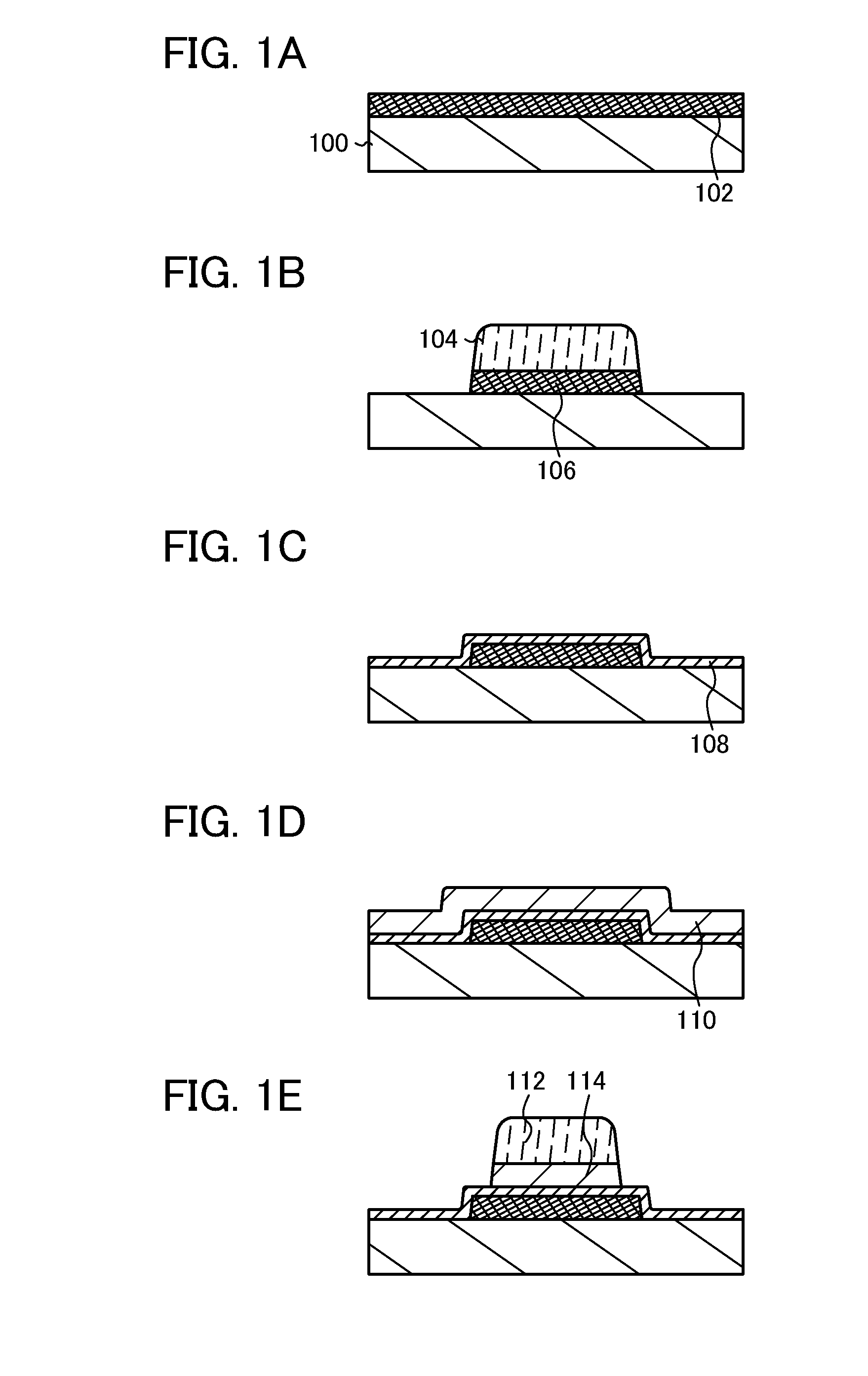
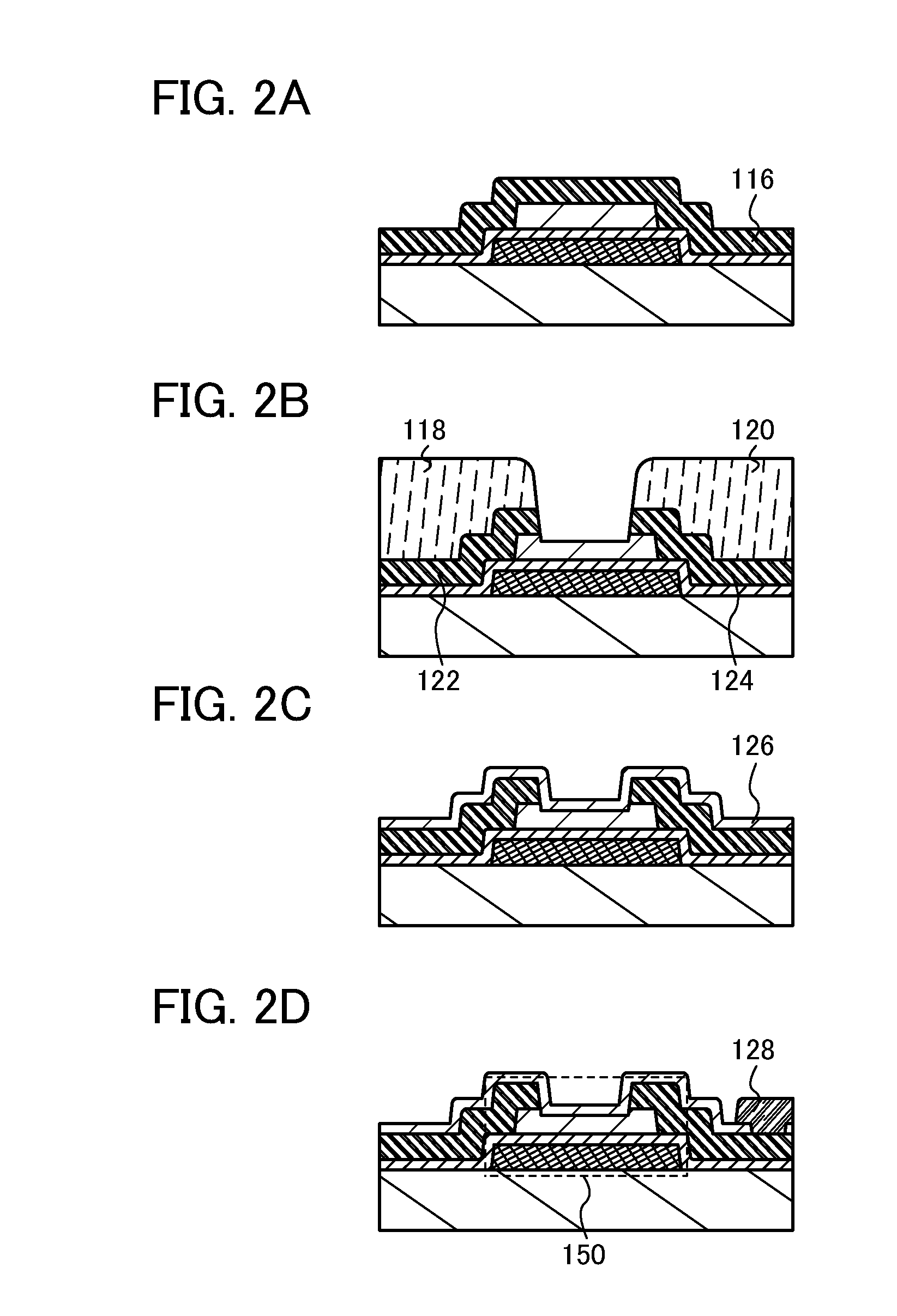
[0046]In this embodiment, an example of a method for manufacturing a semiconductor element which is used for a semiconductor device is described with reference to drawings.

[0047]First, a conductive layer 102 is formed over a substrate 100 (see FIG. 1A).

[0048]Any substrate can be used for the substrate 100 as long as it is a substrate having an insulating surface, for example, a glass substrate. It is preferable that the glass substrate be a non-alkali glass substrate. As a material of the non-alkali glass substrate, a glass material such as aluminosilicate glass, aluminoborosilicate glass, barium borosilicate glass, or the like is used, for example. Besides, as the substrate 100, an insulating substrate formed of an insulator such as a ceramic substrate, a quartz substrate, or a sapphire substrate, a semiconductor substrate formed of a semiconductor material such as silicon, over which an insulating material is covered, a conductive substrate formed of a conductive material such as ...

embodiment 2

[0085]In this embodiment, an example, which is different from the above embodiment, of a method for manufacturing a semiconductor element used for a semiconductor device is described with reference to drawings. Note that many parts of a method for manufacturing a semiconductor device in this embodiment are the same as those in Embodiment 1. Therefore, in the following description, repeated description of the same portions is omitted, and different points are described in detail.

[0086]First, a conductive layer 202 is formed over a substrate 200 (see FIG. 3A). The previous embodiment (the description with reference to FIG. 1A or the like) can be referred to for the details of the substrate 200, the conductive layer 202, or the like. A base layer may be formed over the substrate 200. The previous embodiment can also be referred to for the detail of the base layer.

[0087]Next, a resist mask 204 is selectively formed over the conductive layer 202 and the conductive layer 202 is selectivel...

embodiment 3

[0108]In this embodiment, a manufacturing process of an active matrix substrate which is an example of a semiconductor device is described with reference to drawings. Note that many parts of the manufacturing process described in this embodiment are the same as those in the previous embodiments. Therefore, in the following description, repeated description of the same portions is omitted, and different points are described in detail. Note that in the following description, FIGS. 5A to 5C and FIGS. 6A to 6C are cross-sectional views and FIG. 7 is a plan view. In addition, line A1-A2 and line B1-B2 in each of FIGS. 5A to 5C and FIGS. 6A to 6C correspond to line A1-A2 and line B1-B2 in FIG. 7, respectively. Note also that in this embodiment, a semiconductor element illustrated in a structure taken along line A1-A2 is similar to the semiconductor element described in the previous embodiment (Embodiment 2).

[0109]First, a wiring and an electrode (a gate electrode 302, a capacitor wiring 3...


PUM


Abstract

An object is to provide a semiconductor device including a semiconductor element which has favorable characteristics. A manufacturing method of the present invention includes the steps of: forming a first conductive layer which functions as a gate electrode over a substrate; forming a first insulating layer to cover the first conductive layer; forming a semiconductor layer over the first insulating layer so that part of the semiconductor layer overlaps with the first conductive layer; forming a second conductive layer to be electrically connected to the semiconductor layer; forming a second insulating layer to cover the semiconductor layer and the second conductive layer; forming a third conductive layer to be electrically connected to the second conductive layer; performing first heat treatment after forming the semiconductor layer and before forming the second insulating layer; and performing second heat treatment after forming the second insulating layer.

Description

TECHNICAL FIELD[0001]The technical field relates to a method for manufacturing a semiconductor device.BACKGROUND ART[0002]There are a wide variety of metal oxides and such material oxides are used for various applications. Indium oxide is a well-known material and is used as a transparent electrode material which is necessary for liquid crystal displays and the like.[0003]Some metal oxides have semiconductor characteristics. The examples of such metal oxides having semiconductor characteristics are tungsten oxide, tin oxide, indium oxide, zinc oxide, and the like. A thin film transistor in which a channel formation region is formed using such metal oxides having semiconductor characteristics is known (for example, see Patent Documents 1 to 4, Non-Patent Document 1).[0004]As metal oxides, multi-component oxides as well as single-component oxides are known. For example, homologous compound, InGaO3(ZnO)m (m is natural number) is known as a multi-component oxide containing In, Ga and Zn...

Claims


Application Information

Patent Timeline
Patent Type & Authority Applications(United States)
IPC IPC(8): H01L21/34
CPCC01G15/006C01G45/006C01G49/009C01G51/006C01G53/006C01P2002/52H01L29/66742H01L21/02554H01L21/02565H01L21/02631H01L27/1225H01L29/7869H01L29/66969C01P2006/40H01L21/324H01L21/02164H01L21/02178H01L21/02183H01L21/02266H01L21/441H01L21/477
Inventor OHARA, HIROKISASAKI, TOSHINARI
Owner SEMICON ENERGY LAB CO LTD
Why Eureka
Try Eureka