Electron emitting element, electron emitting device, charging device, image forming apparatus, electron-beam curing device, light emitting device, image display device, air blowing device, and cooling device

a technology of electron emission and electron beam, applied in the field of electron emission element, can solve the problems of inability of thin-film electrode to secure electrical conductivity, uneven thickness of thin-film electrode, and inability to emit electrons through thin-film electrode, so as to achieve greater surface roughness of electron acceleration layer, reduce electron emission, and reduce the effect of electron emission

Active Publication Date: 2010-11-25
SHARP KK
View PDF44 Cites 19 Cited by
  • Summary
  • Abstract
  • Description
  • Claims
  • Application Information

AI Technical Summary

Benefits of technology

[0013]According to the configuration, there is provided, between the electrode substrate and the thin-film electrode, the electron acceleration layer including (i) the insulating fine particles and (ii) at least one of (a) the conductive fine particles having the average particle diameter that is smaller than that of the insulating fine particles and (b) the basic dispersant. This electron acceleration layer is a thin-film layer made up of (i) the insulating fine particles and (ii) at least one of (a) the conductive fine particles and (b) the basic dispersant, which are densely aggregated. The electron acceleration layer has a semiconductive property. When a voltage is applied to the semiconductive electron acceleration layer, current flow occurs in the electron acceleration layer. A part of electrons in the current become ballistic electrons due to an intense electric field produced by the applied voltage and the ballistic electrons are emitted.
[0014]Here, in a case where the electron acceleration layer contains the basic dispersant, it is considered that an electron pair donor that donates a pair of electrons, included in the basic dispersant, causes electrons to be emitted from the electron emitting element. That is, the basic dispersant includes the electron pair donor that donates a pair of electrons, and the electron pair donor is ionized after donating the pair of electrons. It is considered that the ionized electron pair donor transfers electric charge on a surface of each of the insulating fine particles to which the electron pair donor is attached, thereby allowing electrical conduction on the surface of each of the insulating fine particles.
[0015]Further, according to the configuration, the electron acceleration layer has the surface roughness of 0.2 μm or less in centerline average roughness (Ra), and the thin-film electrodes has the film thickness of 100 nm or less.
[0016]In a case of forming the thin-film electrode by sputtering as described earlier, the thin-film electrode has a thin thickness in a concave portion while it has a thick thickness in a convex portion. For the thin-film electrode having a thin film thickness, the concave and convex portions of the surface are enhanced so that the convex portion is in a form of island. Accordingly, the surface of the thin-film electrode becomes no longer conductive. In order to absorb such surface roughness on the surface of the electron acceleration layer so that the surface of the thin-film electrode becomes conductive, it is necessary to increase the film thickness of the thin-film electrode. That is, the thin-film electrode needs to be thicker than an electrode to be provided on a plane surface. As is clear from the above description, the thin-film electrode needs to be thicker as the surface roughness of the electron acceleration layer becomes greater. However, the thin-film electrode having a thick film thickness allows a smaller amount of electrons to be emitted through the thin-film electrode. As such, the electron emission is reduced.
[0017]In contrast, according to the above configuration, the surface roughness of the electron acceleration layer is optimized, i.e., the surface roughness of the electron acceleration layer is 0.2 μm or less in centerline average roughness (Ra). This makes it possible to reduce the thickness of the thin-film electrode to an appropriate thickness, i.e., 100 nm or less. The thin-film electrode having a too thick film thickness indeed achieves conductivity on the surface of the element; however, it reduces an amount of the electrons being emitted through the thin-film electrode. Therefore, the film thickness of the thin-film electrode is preferably 100 nm or less.
[0018]As such, according to the electron emitting element of the present invention, it is possible to optimize the surface roughness of the electron acceleration layer, and to reduce the thickness of the thin-film electrode to the appropriate thickness. Accordingly, it is possible to increase the electron emission.

Problems solved by technology

However, such a thickness of 0.1 μm or greater hinders the electrons from being emitted through the thin-film electrode.
However, if the thin-film electrode is provided on the surface of the electron acceleration layer, a thickness of the thin-film electrode becomes uneven.
In a case where the thin-film electrode has a too thin thickness, the thin-film electrode cannot secure electrical conductivity.
Accordingly, it is not possible to allow a sufficient electrical current to pass through the element.
In addition, the element becomes weaker in strength.
On the other hand, in a case where the thin-film electrode has a too thick thickness, the thin-film electrode has a difficulty of emitting the electrons therefrom.
However, according to the electron emitting elements of Patent Literature 1, the thickness of the thin-film electrode is not optimized in consideration of the surface roughness of the surface of the emitter section.

Method used


Image

  • Electron emitting  element, electron emitting device, charging device, image forming apparatus, electron-beam curing device, light emitting device, image display device, air blowing device, and cooling device
  • Electron emitting  element, electron emitting device, charging device, image forming apparatus, electron-beam curing device, light emitting device, image display device, air blowing device, and cooling device
  • Electron emitting  element, electron emitting device, charging device, image forming apparatus, electron-beam curing device, light emitting device, image display device, air blowing device, and cooling device

Examples


embodiment 1

Configuration of Element

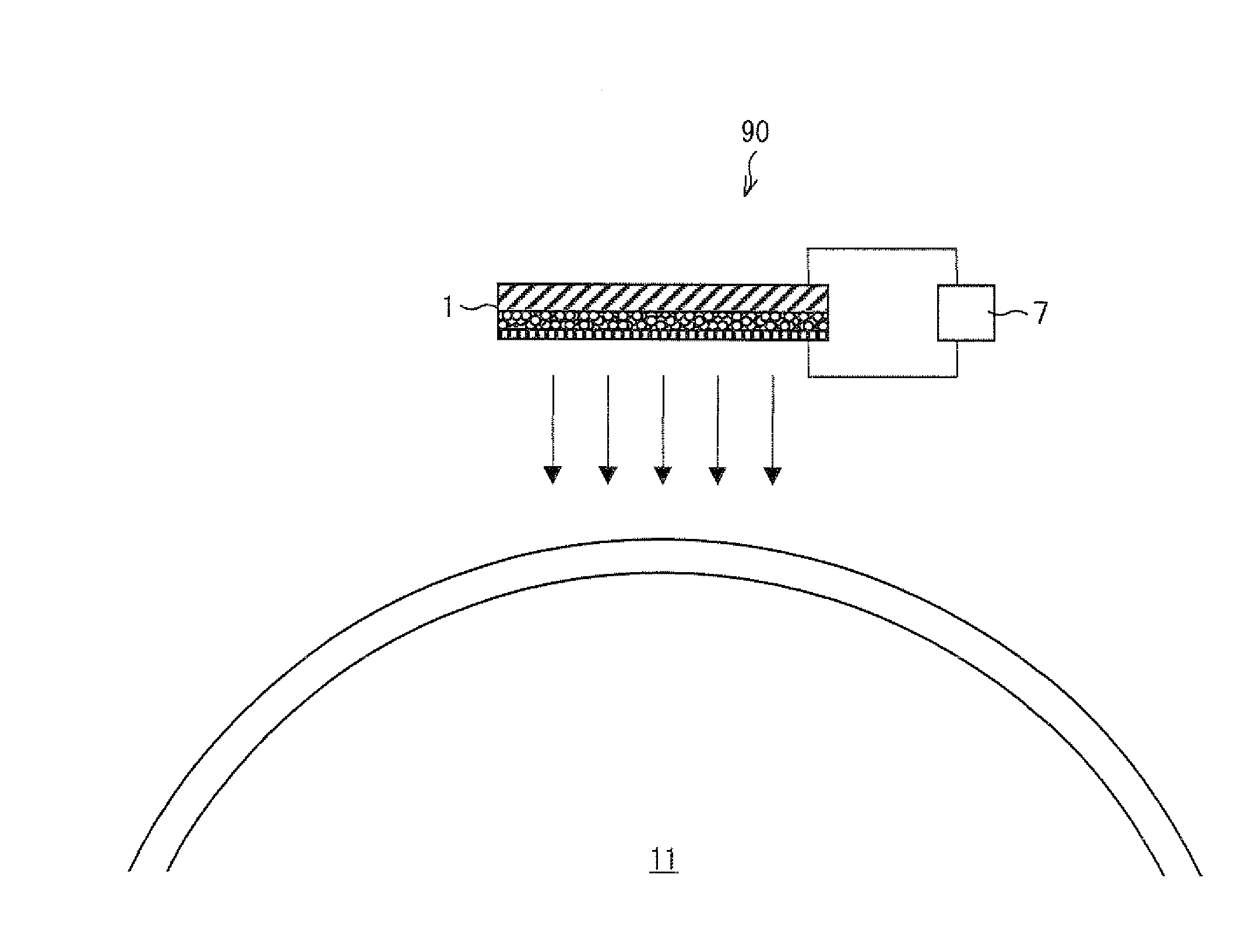
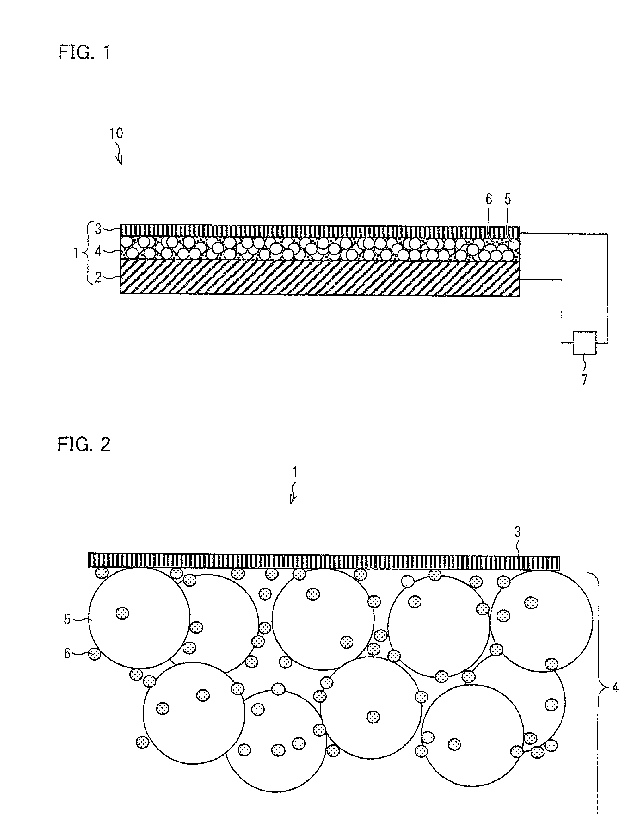
[0046]FIG. 1 is a schematic view illustrating a configuration of an electron emitting device 10 including an electron emitting element 1 according to one embodiment of the present invention. As shown in FIG. 1, the electron emitting device 10 includes the electron emitting element 1 according to one embodiment of the present invention, and a power supply 7. As shown in FIG. 1, the electron emitting element 1 of the present embodiment includes: an electrode substrate 2 as a lower electrode; a thin-film electrode 3 as an upper electrode; and an electron acceleration layer 4 sandwiched therebetween. Further, the electrode substrate 2 and the thin-film electrode 3 are connected to the power supply 7, so that a voltage can be applied between the electrode substrate 2 and the thin-film electrode 3 which are provided so as to face each other. The electron emitting element 1 applies a voltage between the electrode substrate 2 and the thin-film electrode 3 so that cur...

example 1

[0087]First, (i) 3 mL of toluene solvent, serving as a dispersion solvent, and (ii) 0.5 g of spherical silica particles (average particle diameter: 50 nm), serving as insulating fine particles 5, were supplied into a 10 mL reagent bottle. The reagent bottle was stirred by using an ultrasonic dispersion device for 30 minutes so as to disperse the spherical silica particles. Next, 0.125 g of silver nanoparticles made by Applied Nano Particle Laboratory Co. (average particle diameter of silver nanoparticles: 10 nm (including 1 nm of an alcoholate insulating film which coats the silver nanoparticles)), serving as conductive fine particles 6, were additionally supplied to the reagent bottle, and then the reagent bottle was subjected to the ultrasonic dispersion process as above. In this way, a fine particle dispersion solution “a”, in which the spherical silica particles and the silver nanoparticles were dispersed, was obtained. The ultrasonic dispersion process, which was carried out af...

example 2

[0091]An electron acceleration layer 4 was produced in a same manner as in Example 1, except that a period of the ultrasonic dispersion process after the silver nanoparticles were added was 30 minutes. A surface of the electron acceleration layer 4 of Example 2 was observed under the laser microscope, and found to have Ra of 0.2 μm.

[0092]In Example 2, a plurality of electron acceleration layers 4 were produced. Then, thin-film electrodes 3, each of which was made of gold and had the surface area of 0.014 cm2, were formed on surfaces of the respective plurality of electron acceleration layers 4. The thin-film electrodes 3 thus formed had film thicknesses of 5 μm, 10 μm, 15 μm, 30 μm, 35 μm, 40 μm, and 45 μm, respectively. As such, a plurality of electron emitting elements of Example 2 were obtained.

[0093]FIG. 5 illustrates measurement results, of electron emission current per unit area, measured for each of the plurality of electron emitting elements under vacuum of 1×10⁻⁸ ATM.

[0094]...


PUM


Abstract

According to an electron emitting element of the present invention, an electron acceleration layer sandwiched between an electrode substrate and a thin-film electrode contains (i) insulating fine particles and (ii) at least one of (a) conductive fine particles having an average particle diameter smaller than an average particle diameter of the insulating fine particles and (b) a basic dispersant. The electron acceleration layer has a surface roughness of 0.2 μm or less in centerline average roughness (Ra). The thin-film electrode has a film thickness of 100 nm or less. As such, according to the electron emitting element of the present invention, it is possible to reduce the thickness of the thin-film electrode to an appropriate thickness. Accordingly, it is possible to increase electron emission.

Description

[0001]This Nonprovisional application claims priority under 35 U.S.C. §119(a) on Patent Application No. 2009-121456 filed in Japan on May 19, 2009, the entire contents of which are hereby incorporated by reference.TECHNICAL FIELD[0002]The present invention relates to an electron emitting element for emitting electrons by application of a voltage.BACKGROUND ART[0003]A Spindt-type electrode and a carbon nanotube electrode (CNT) have been known as conventional electron emitting elements. Applications of such conventional electron emitting elements to, for example, the field of Field Emission Display (FED) have been studied. Such electron emitting elements are caused to emit electrons by tunnel effect resulting from formation of an intense electric field of approximately 1 GV / m that is produced by application of a voltage to a pointed section.[0004]However, each of these two types of the electron emitting elements has an intense electric field in the vicinity of a surface of an electron...

Claims


Application Information

Patent Timeline
Patent Type & Authority Applications(United States)
IPC IPC(8): G03G15/02H01J1/02H05B41/00H01T23/00H02B1/56
CPCB82Y10/00H01J2201/3125H01J1/312G03G15/02
Inventor IMURA, YASUOHIRAKAWA, HIROYUKINAGAOKA, AYAEIWAMATSU, TADASHI
Owner SHARP KK
Why Eureka
Try Eureka