Group iii nitride semiconductor epitaxial substrate and method for manufacturing the same

a technology of nitride and semiconductor, applied in the direction of semiconductor laser, final product manufacturing, sustainable manufacturing/processing, etc., can solve the problems of deterioration of device characteristics, affecting the quality of alsub>x/sub>ga/sub>n (0x1) crystals, and affecting the quality of alsub>x/sub>ga/sub>1-x/sub>n (0x1) crystals,

Inactive Publication Date: 2010-12-30
SHOWA DENKO KK
View PDF2 Cites 89 Cited by
  • Summary
  • Abstract
  • Description
  • Claims
  • Application Information

AI Technical Summary

Benefits of technology

[0016]As described above, according to the group III nitride semiconductor epitaxial substrate and the manufacturing method thereof of the present invention, a group III nitride semiconducto

Problems solved by technology

With respect to such devices for emitting or receiving light in the ultraviolet or deep ultraviolet region, in those cases where either a template substrate in which a GaN layer is laminated on top of a substrate composed of a single crystal of different kinds such as sapphire or SiC, or an independent GaN substrate is used in a conventional manner, light emitted from a light emitting layer is absorbed by the GaN layer, which is a problem.
Further, in those cases where an AlGaN layer having a high ratio of Al composition is deposited on a GaN layer, cracks are formed due to the differences in the lattice constant and the coefficient of thermal expansion, thereby causing deterioration in the device characteristics.
However, the quality of AlxGa1-xN (0

Method used


Image

  • Group iii nitride semiconductor epitaxial substrate and method for manufacturing the same
  • Group iii nitride semiconductor epitaxial substrate and method for manufacturing the same
  • Group iii nitride semiconductor epitaxial substrate and method for manufacturing the same

Examples


example 1

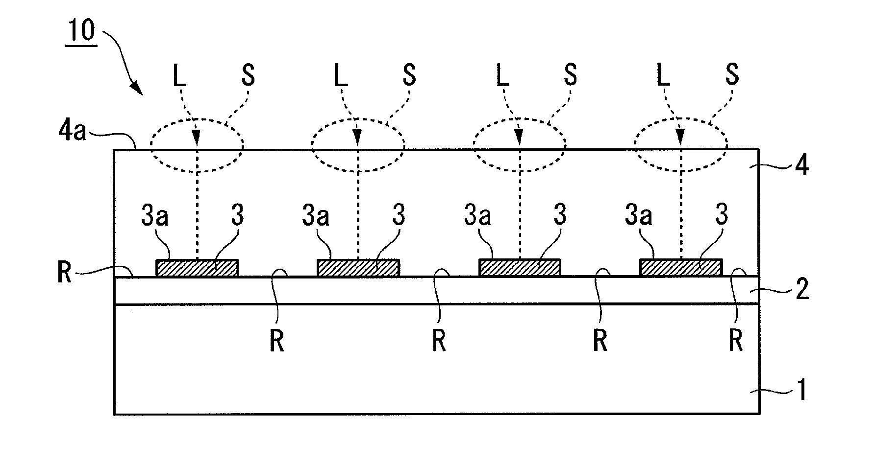
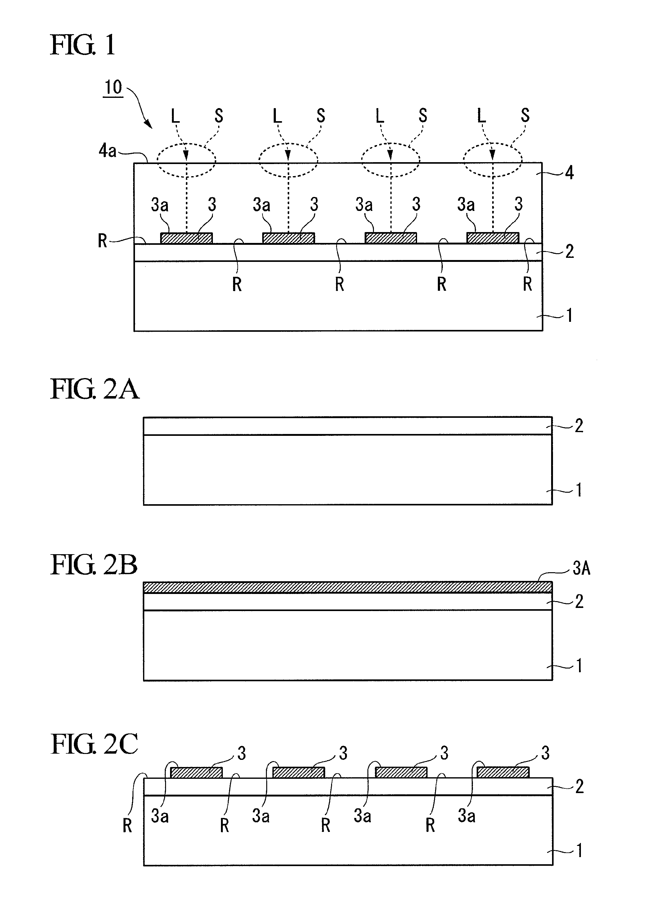
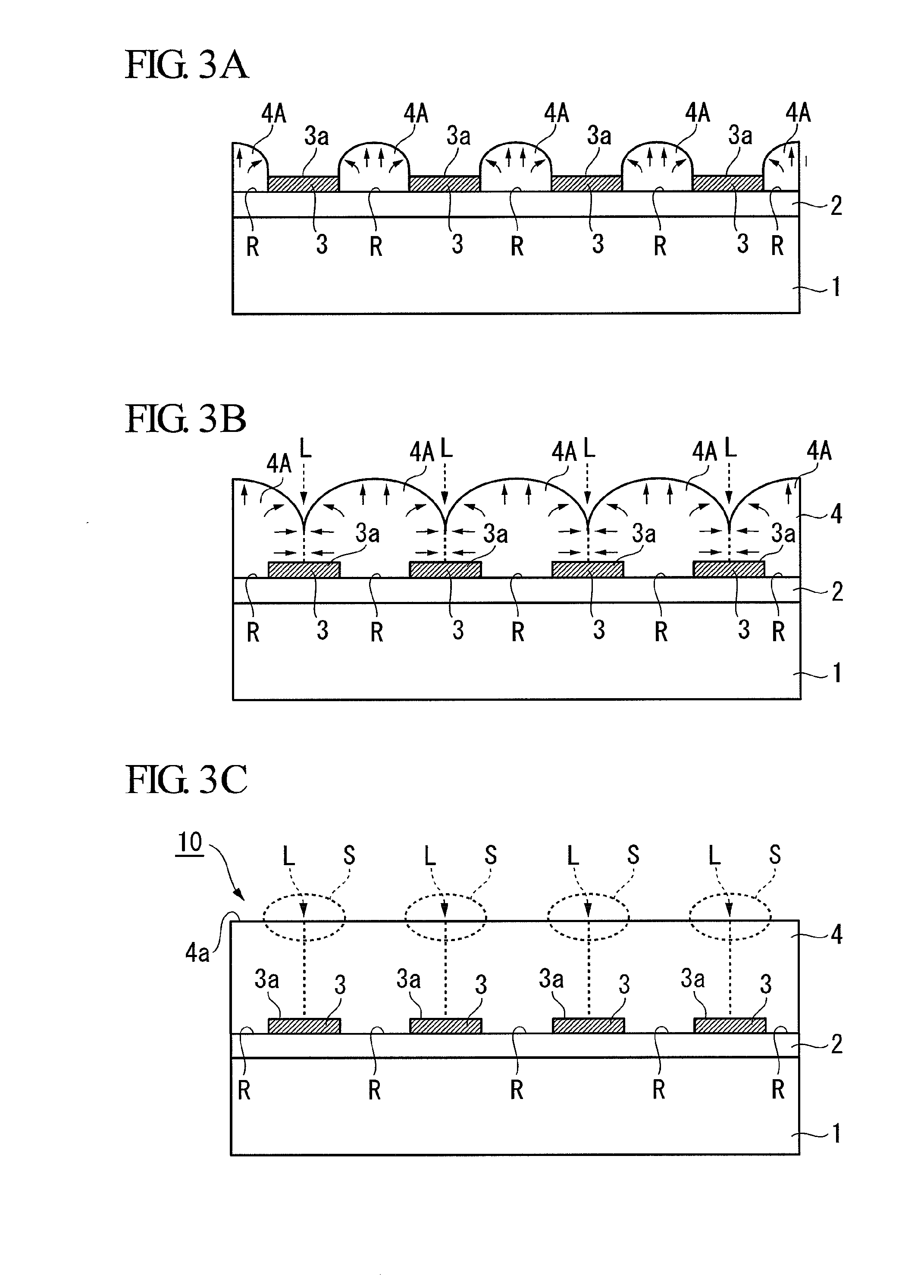
[0068]An AlN epitaxial substrate having a structure as shown in FIG. 1 was manufactured by the method as shown below.

(Group III Nitride Layer Forming Step)

[0069]An AlN film to be served as a group III nitride layer was first formed on top of a sapphire substrate. A high-temperature MOCVD apparatus was used for AlN formation. More specifically, a sapphire substrate was mounted on a molybdenum susceptor, and the substrate was set inside a water-cooled reactor made of stainless steel via a load lock chamber. Thereafter, nitrogen gas was caused to flow through for purging inside the reaction furnace.

[0070]Next, after replacing the gas flowing through inside the MOCVD furnace with hydrogen gas, the pressure inside the reactor was maintained at 30 ton. The substrate temperature was increased from room temperature to 1,400° C. over 15 minutes using an electrical resistance heater. Subsequently, while retaining the substrate temperature at 1,400° C., hydrogen gas was caused to flow through ...


PUM

PropertyMeasurementUnit
Compositionaaaaaaaaaa
Semiconductor propertiesaaaaaaaaaa

Abstract

There is provided a group III nitride semiconductor epitaxial substrate which has a suppressed level of threading dislocation in the vertical direction and excellent crystal quality, the group III nitride semiconductor epitaxial substrate including a substrate (1) for growing an epitaxial film; and an ELO layer (4) having a composition of AlxGa1-xN (0≦x≦1) formed either on top of the substrate (1) or on top of a group III nitride layer (2) formed on top of the substrate (1), wherein the ELO layer (4) is a layer formed by using a mask pattern (3), which is composed of carbon and is formed either on top of the substrate (1) or on top of the group III nitride layer (2).

Description

TECHNICAL FIELD[0001]The present invention relates to a group III nitride semiconductor epitaxial substrate and an improved method for manufacturing the same.[0002]Priority is claimed on Japanese Patent Application No. 2008-029456, filed Feb. 8, 2008, the content of which is incorporated herein by reference.BACKGROUND ART[0003]Applications of group III nitride semiconductor devices and in particular, devices for emitting or receiving light having a wavelength of 360 nm or less in the ultraviolet or deep ultraviolet region which use AlxGa1-xN (0<x≦1) substrates have been anticipated for some time in the field of medical treatments or precision machining.[0004]With respect to such devices for emitting or receiving light in the ultraviolet or deep ultraviolet region, in those cases where either a template substrate in which a GaN layer is laminated on top of a substrate composed of a single crystal of different kinds such as sapphire or SiC, or an independent GaN substrate is used i...

Claims


Application Information

Patent Timeline
IPC IPC(8): C09K11/64H01L21/20C23C16/04C23C16/34C30B25/04C30B29/38H01L21/205H01L31/10H01L33/16H01L33/32H01S5/02
CPCC30B25/02C30B29/403H01L21/0237H01L21/02458H01L21/0254H01L21/0262Y02E10/544H01L21/02647H01L31/03048H01L31/1844H01L33/0075H01S5/32341H01S2304/12H01L21/02642Y02P70/50
Inventor BANDO, AKIRAAMANO, HIROSHI
Owner SHOWA DENKO KK
Why Eureka
Try Eureka