Sputtering target and manufacturing method thereof, and transistor

a technology of sputtering target and manufacturing method, which is applied in the direction of diaphragms, metal-working apparatus, metallic material coating process, etc., can solve the problems of difficult control of degradation over time, insufficient characteristics of a semiconductor element manufactured using an oxide semiconductor, etc., and achieve high-reliability semiconductor effects

Inactive Publication Date: 2011-05-19
SEMICON ENERGY LAB CO LTD
View PDF99 Cites 34 Cited by
  • Summary
  • Abstract
  • Description
  • Claims
  • Application Information

AI Technical Summary

Benefits of technology

[0025]In one embodiment of the present invention, a sputtering target containing a small amount of impurities such as a compound containing a hydrogen atom typified by H2O or a hydrogen atom can be provided. An oxide semiconductor film

Problems solved by technology

However, characteristics of a semiconductor element which is manufactured using an oxide semiconductor are not yet sufficient.
In a transistor manufactured using an oxide semiconductor film co

Method used


Image

  • Sputtering target and manufacturing method thereof, and transistor
  • Sputtering target and manufacturing method thereof, and transistor
  • Sputtering target and manufacturing method thereof, and transistor

Examples


embodiment 1

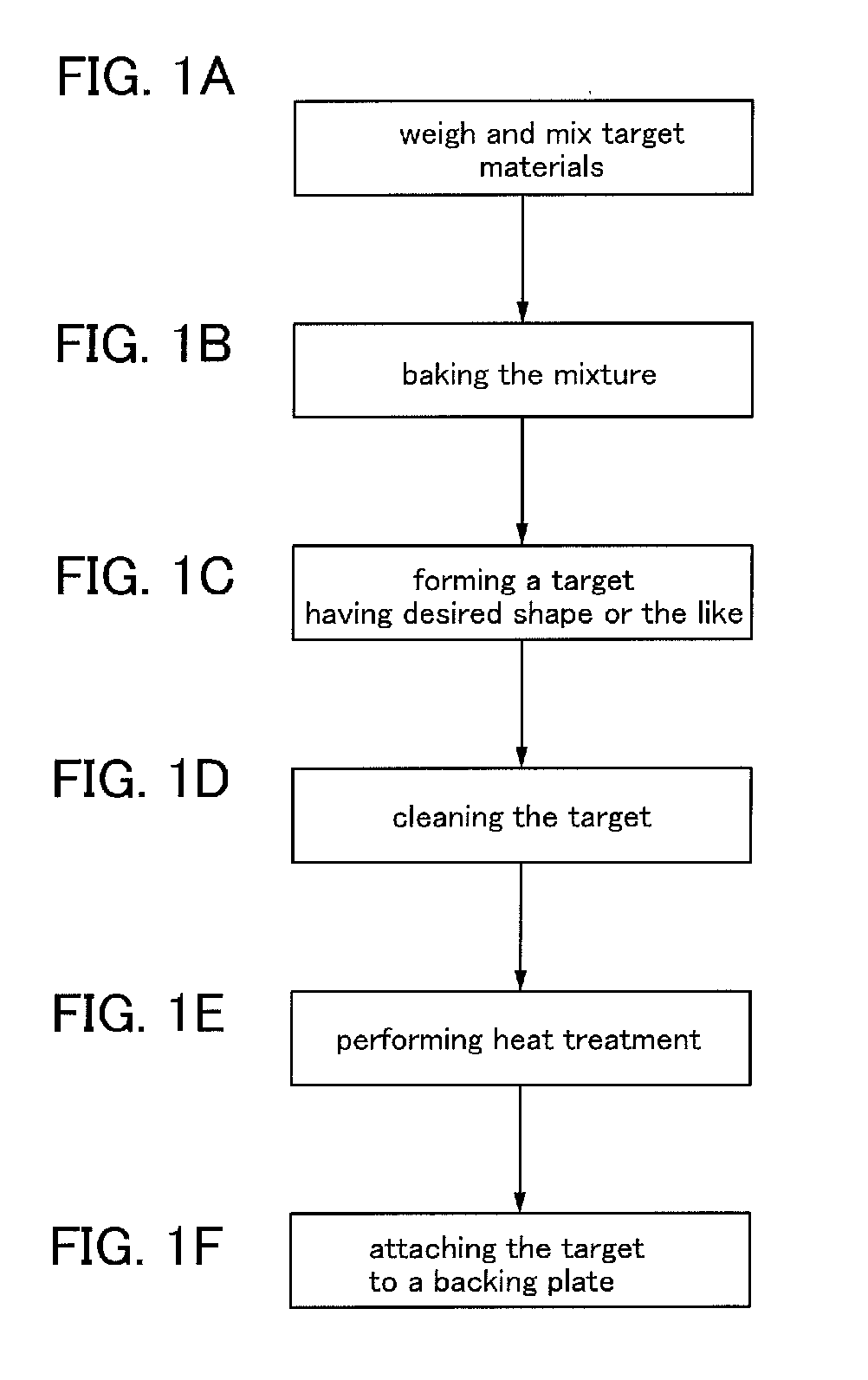
[0043]In this embodiment, a manufacturing method of a sputtering target (hereinafter, also referred to as a target) which is one embodiment of the present invention will be described with reference to FIGS. 1A to 1F. FIGS. 1A to 1F are a flow chart illustrating an example of a manufacturing method of a sputtering target according to this embodiment.

[0044]First, target materials are weighed as appropriate, and the weighed target materials are mixed, while each being crushed by a ball mill or the like. As target materials for forming an oxide semiconductor film, for example, magnesium oxide, zinc oxide, aluminum oxide, gallium oxide, indium oxide, tin oxide, and the like may be mixed as appropriate (FIG. 1A).

[0045]Further, silicon oxide may be added to the target at 2 wt % to 10 wt % inclusive, so that SiOX (X>0) is included in the oxide semiconductor film. When an oxide semiconductor film includes SiOX (X>0), crystallization of the oxide semiconductor film can be inhibited.

[0046]In t...

embodiment 2

[0066]In this embodiment, an example of manufacturing a transistor as a semiconductor device which is manufactured using the target in Embodiment 1 will be described. In a transistor 410 described in this embodiment, an oxide semiconductor film which is formed using the sputtering target described in Embodiment 1 can be used as an active layer.

[0067]One embodiment of a transistor and one embodiment of a manufacturing method of the transistor of this embodiment are described with reference to FIGS. 2A and 2B and FIGS. 3A to 3E.

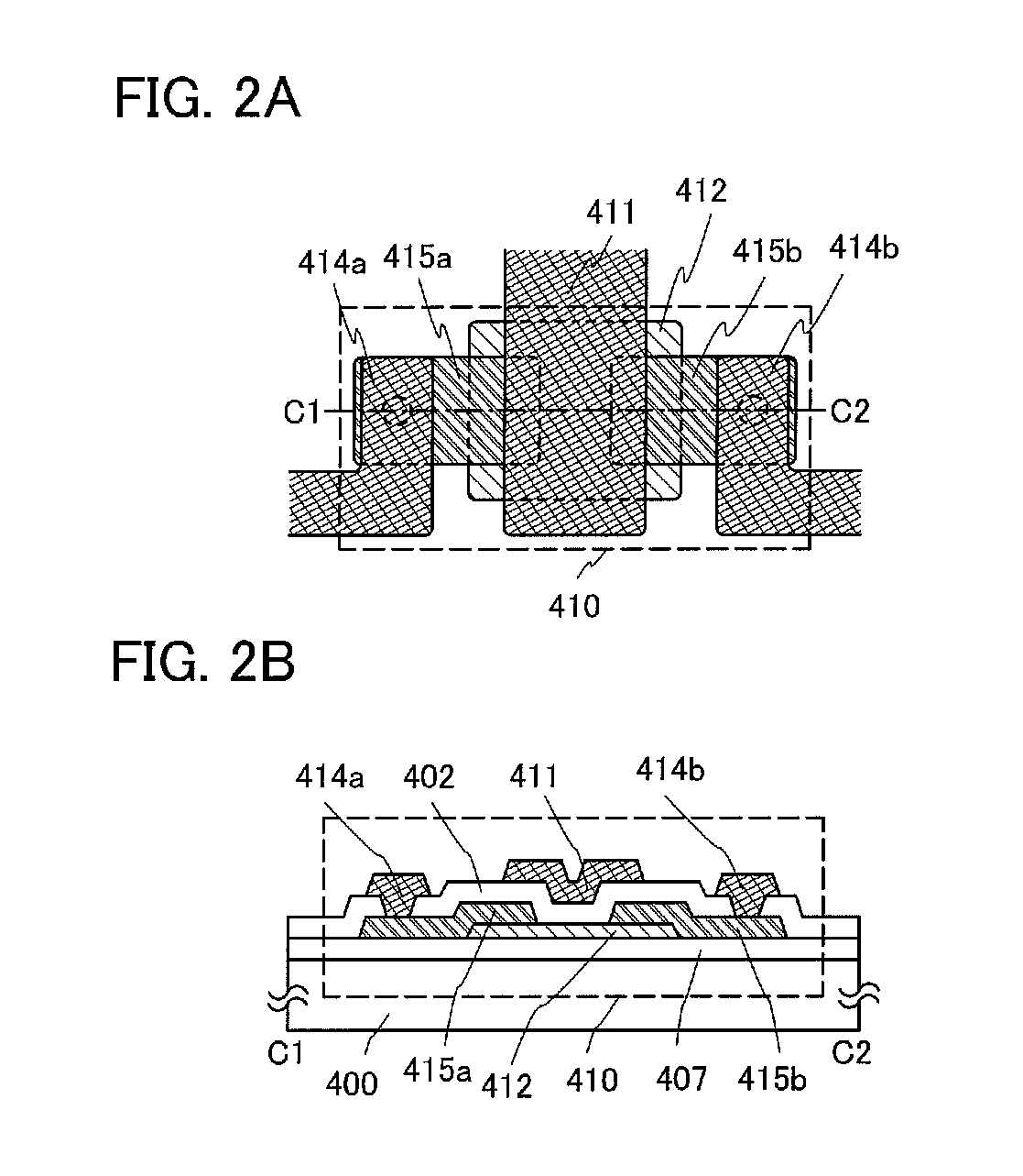
[0068]An example of a plan structure and an example of a cross-sectional structure of a transistor are respectively illustrated in FIGS. 2A and 2B. The transistor 410 illustrated in FIGS. 2A and 2B is one of top-gate transistors.

[0069]FIG. 2A is a plan view of the top-gate transistor 410 and FIG. 2B is a cross-sectional view taken along line C1-C2 in FIG. 2A.

[0070]The transistor 410 includes an oxide semiconductor layer 412, a source or drain electrode layer 41...

embodiment 3

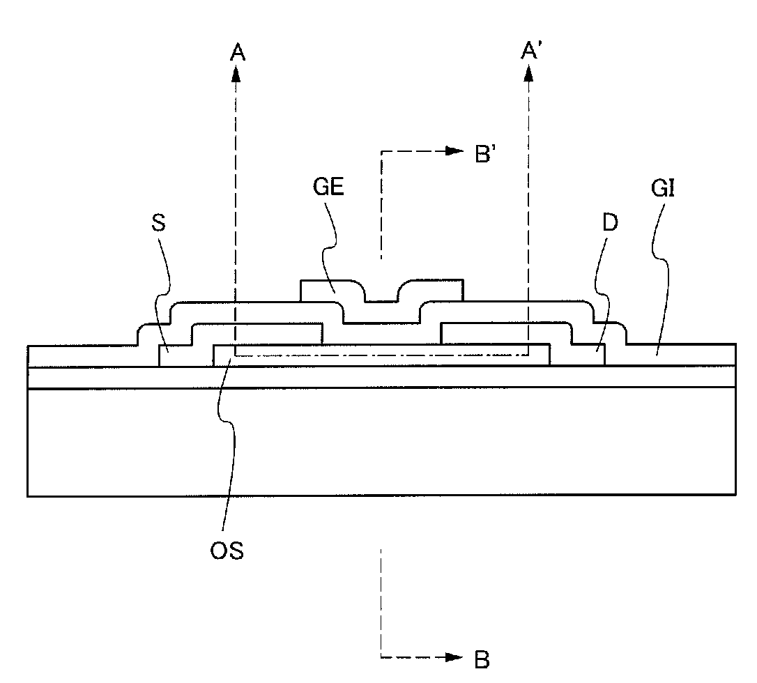
[0170]In this embodiment, an example of manufacturing a transistor as a semiconductor device which is manufactured using the target in Embodiment 1 will be described. Note that the same portions as in Embodiment 2 or portions having functions similar to those in Embodiment 2, and steps for forming such portions may be similar to those in Embodiment 2, and repetitive description thereof will be omitted. In addition, detailed description of the same portions is not repeated. In a transistor 460 described in this embodiment, an oxide semiconductor film which is formed using the sputtering target described in Embodiment 1 can be used as an active layer.

[0171]One embodiment of a transistor and one embodiment of a method for manufacturing the transistor in this embodiment will be described with reference to FIGS. 4A and 4B and FIGS. 5A to 5E.

[0172]An example of a plan structure and a cross-sectional structure of a transistor are illustrated in FIGS. 4A and 4B, respectively. The transistor...


PUM

PropertyMeasurementUnit
Temperatureaaaaaaaaaa
Fractionaaaaaaaaaa

Abstract

One object is to provide a deposition technique for forming an oxide semiconductor film. By forming an oxide semiconductor film using a sputtering target including a sintered body of a metal oxide whose concentration of hydrogen contained is low, for example, lower than 1×10¹⁶ atoms/cm3, the oxide semiconductor film contains a small amount of impurities such as a compound containing hydrogen typified by H2O or a hydrogen atom. In addition, this oxide semiconductor film is used as an active layer of a transistor.

Description

TECHNICAL FIELD[0001]The present invention relates to a sputtering target and a manufacturing method thereof. In addition, the present invention relates to a transistor manufactured using the sputtering target.BACKGROUND ART[0002]A transistor formed over a flat plate such as a glass substrate, which is typically used in a liquid crystal display device, is generally formed using a semiconductor material such as amorphous silicon or polycrystalline silicon. A transistor manufactured using amorphous silicon has low field effect mobility, but can be formed over a larger glass substrate. In contrast, a transistor manufactured using polycrystalline silicon has high field effect mobility, but needs a crystallization step such as laser annealing and is not always suitable for a larger glass substrate.[0003]Thus, a technique in which a transistor is manufactured using an oxide semiconductor as a semiconductor material and applied to an electronic device or an optical device has attracted att...

Claims


Application Information

Patent Timeline
IPC IPC(8): H01L29/786C23C14/34B24B1/00B32B38/00B32B38/16
CPCC04B35/01H01L29/66742C04B35/645C04B35/6455C04B41/0072C04B41/009C04B41/80C04B2111/00844C04B2235/3284C04B2235/3286C04B2235/3418C04B2235/658C04B2235/662C04B2235/666C04B2235/77C23C14/10C23C14/3414C23C14/564H01L21/0242H01L21/02422H01L21/02488H01L21/02554H01L21/02565H01L21/02631H01L29/41733H01L29/42384H01L29/45H01L29/78618H01L29/7869C04B35/453H01L29/66969B29C31/008C04B35/04C04B35/10C04B35/457C04B41/4517C04B41/53H01J37/3429H01J2237/332
Inventor YAMAZAKI, SHUNPEITAKAYAMA, TORUSATO, KEIJI
Owner SEMICON ENERGY LAB CO LTD
Why Eureka
Try Eureka