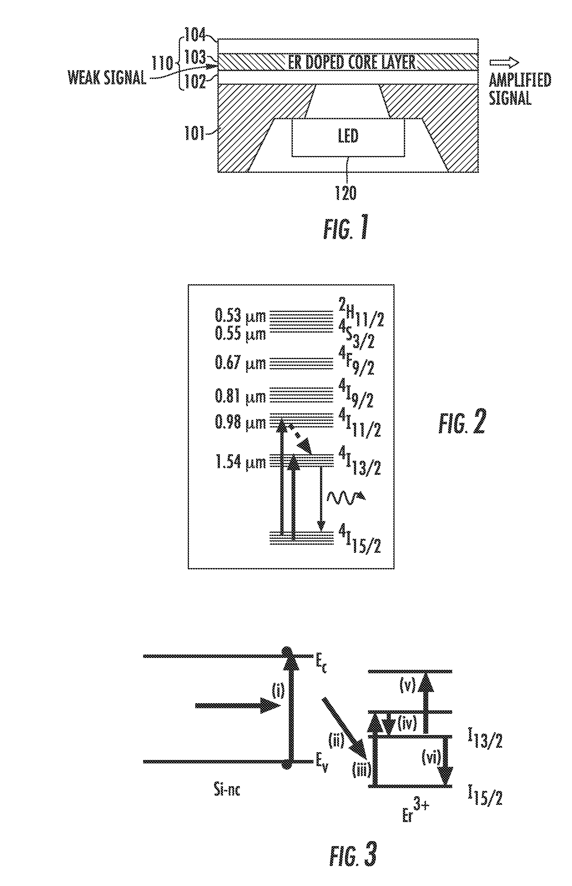
[0018]An integrated electrically pumped
light emitting device, otherwise definable as an electroluminescent device, within a passive, undoped low-loss
waveguide for optical interconnections in the same
chip or among distinct chips may be provided. The
light emitting device, directly integrated in the passive
waveguide, addresses
coupling problems of the emitting device with the signal conveying / distributing passive waveguide. The structure allows generation of an optical signal directly in the guide, and thus may avoid
coupling losses as occurring in side emission devices III-V, coupled to
silicon oxide waveguides. Indeed, such coupling losses have so far limited the development of optical interconnections.
[0020]To obtain these results, it may be desirable that techniques and
doping conditions used for forming the structure be such to produce the required inversion of the
population of the optically-active
dopant ions, e.g. of
Erbium, in the active region created in the passive waveguide. Moreover, it may be desirable that the electrical field applied for pumping be precisely balanced and not imply significant losses. If these conditions are met the device may attain a net
gain. Even when using the device for amplifying an optical signal, the structure of the integrated
optically active device in a passive waveguide reduces coupling losses.
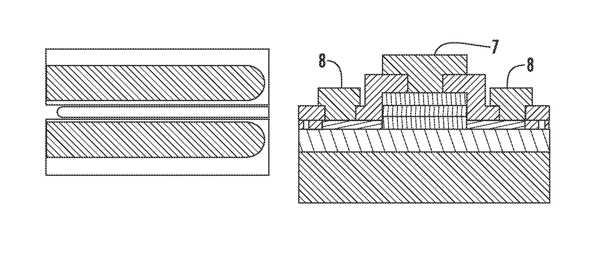
[0022]Such a of “slot” waveguide formed with an
active layer of
oxide or of
silicon nitride, including
silicon nanocrystals (SRO), of particularly small thickness (≦70 nm and preferably ≦50 nm), between
layers of higher refraction index of undoped amorphous or
polycrystalline silicon (polysilicon) is generally compatible with common
CMOS integration technology. For the formatting of the electroluminescent waveguide device to an
optically active portion of SRO doped with
Erbium, locally doped portions of the two silicon layers of relatively high refraction index are also similarly associated, such to locally confer the silicon an appropriate electrical
conductivity, forming the two plates of a typical MOS structure, electrically coupled to the opposite surfaces of the
optically active portion doped with
Erbium (SRO+Er) of the thin core layer. By applying a
voltage on the two plates of the MOS structures it is possible to force an
electric current through the thin optically active portion of the core doped with Erbium (SRO+Er), effectively electrically pumping the so composed electroluminescent device.
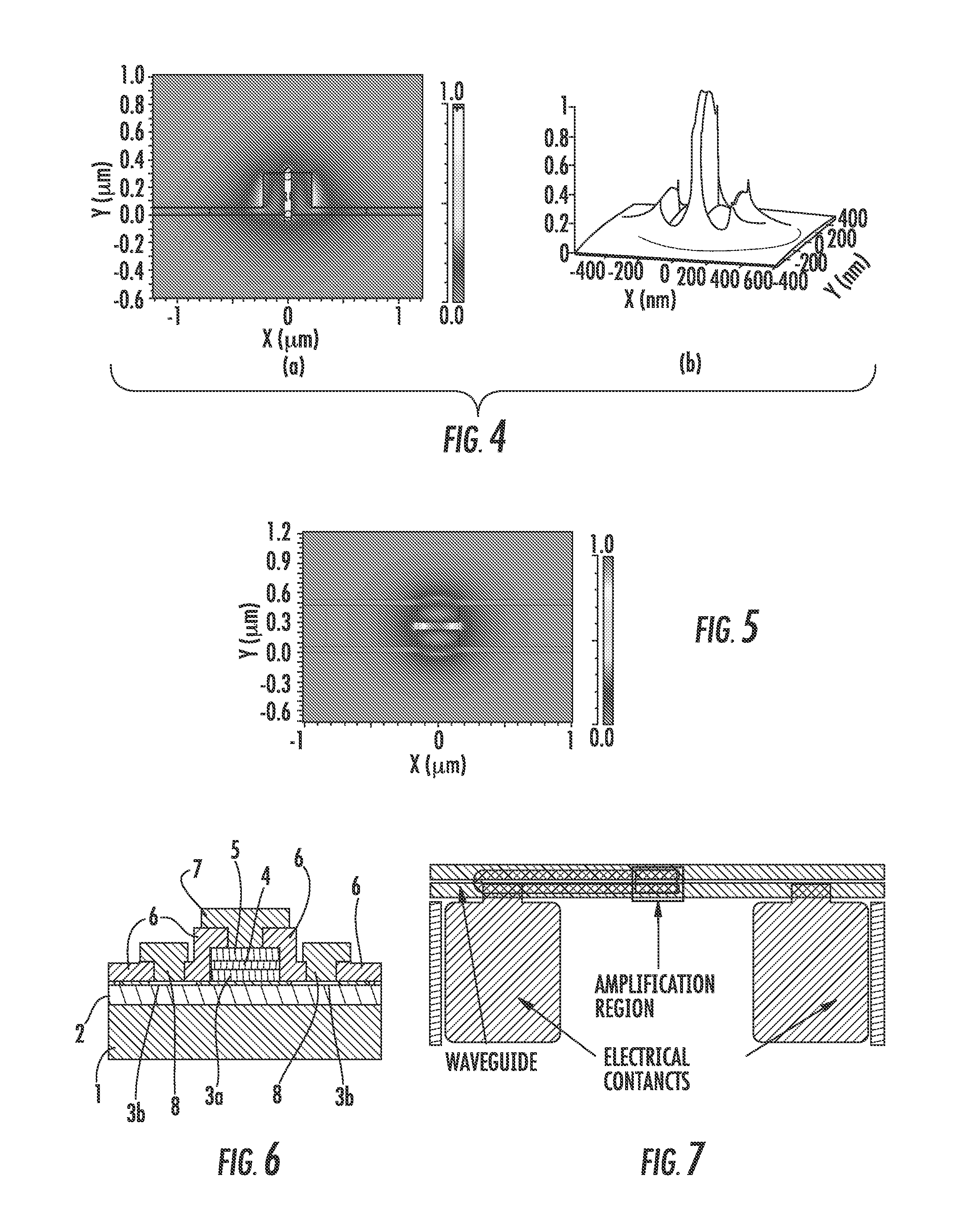
[0023]A extraordinary
strong interaction between the electro-optic active media and the
electromagnetic field is conveyed through the waveguide by virtue of the high confinement factor in the thin low refraction index region and reduction of losses along the guiding structure of an optical signal. By properly choosing the
doping and the thermal budget, and the structure of coupled plates of a MOS structure, an optical signal that propagates in the waveguide and that may be used as a
clock signal is generated. Generally only the electro-optically active portion or region of the optically
active layer of low refraction index of the
slot waveguide is doped with Erbium reducing absorption losses of
Erbium ions, and leaving undoped passive portions of the guiding structure. The device may even function as an electrically pumped
optical amplifier of a signal propagated in the passive guide provided that the Erbium concentration and distribution is adapted to inversion of the
ion population and losses kept sufficiently small not to jeopardize a net
gain of the electrically pumped device.
[0025]According to an embodiment, a further important reduction of optical losses may be obtained, by management of the related thermal budgets, by favoring a dense
population of
silicon nanocrystals in a core array film, for example, of sub-stoichiometric
silicon oxide, limitedly and / or selectively in the optically active portion of the thin low
refractive index core layer of the waveguide doped with Erbium. Indeed, silicon
oxide has an
attenuation coefficient of an optical signal smaller than that of silicon rich silicon oxide, in which silicon nanocrystals are present.

