Pellicle for lithography

a lithography and pellicle technology, applied in the field of pellicle for lithography, can solve the problems of solid-like foreign materials, affecting the performance of the mother substrate and the yield ratio of the semiconductor wafer or the liquid crystal display panel mother substrate is inevitably reduced, so as to achieve the effect of suppressing the degradation of an agglutinant agen

Active Publication Date: 2011-06-02
SHIN ETSU CHEM IND CO LTD
View PDF8 Cites 6 Cited by
  • Summary
  • Abstract
  • Description
  • Claims
  • Application Information

AI Technical Summary

Benefits of technology

[0019]It is therefore an object of the present invention to provide a pellicle for lithography which generates only a small amount of decomposition gas even when the pellicle is used for a long time, thereby preventing

Problems solved by technology

As a result, the pattern of the photomask cannot be transferred onto the semiconductor wafer or the liquid crystal display panel mother substrate in the desired manner and the performance of the semiconductor wafer or the liquid crystal display panel mother substrate is lowered, whereby the yield ratio of the semiconductor wafer or the liquid crystal display panel mother substrate is inevitably reduced.
However, even in such a case, since it is extremely difficult to completely prevent foreign materials from attaching to the surface of the photomask, the operation of exposing the semiconductor wafer or the liquid crystal display panel mother substrate is usually conducted with a dust proof cover, called a pellicle, and having a high transmittance with respect to the exposure light, mounted on the surface of the photomask.
It is considered that this problem of solid-like foreign materials gradually separating out on the pattern region of the photomask surrounded by the pellicle in the case where the photomask on which the pellicle is mounted is exposed for a long time is caused by the presence of ionic residue on t

Method used


Image

  • Pellicle for lithography
  • Pellicle for lithography

Examples


working example 1

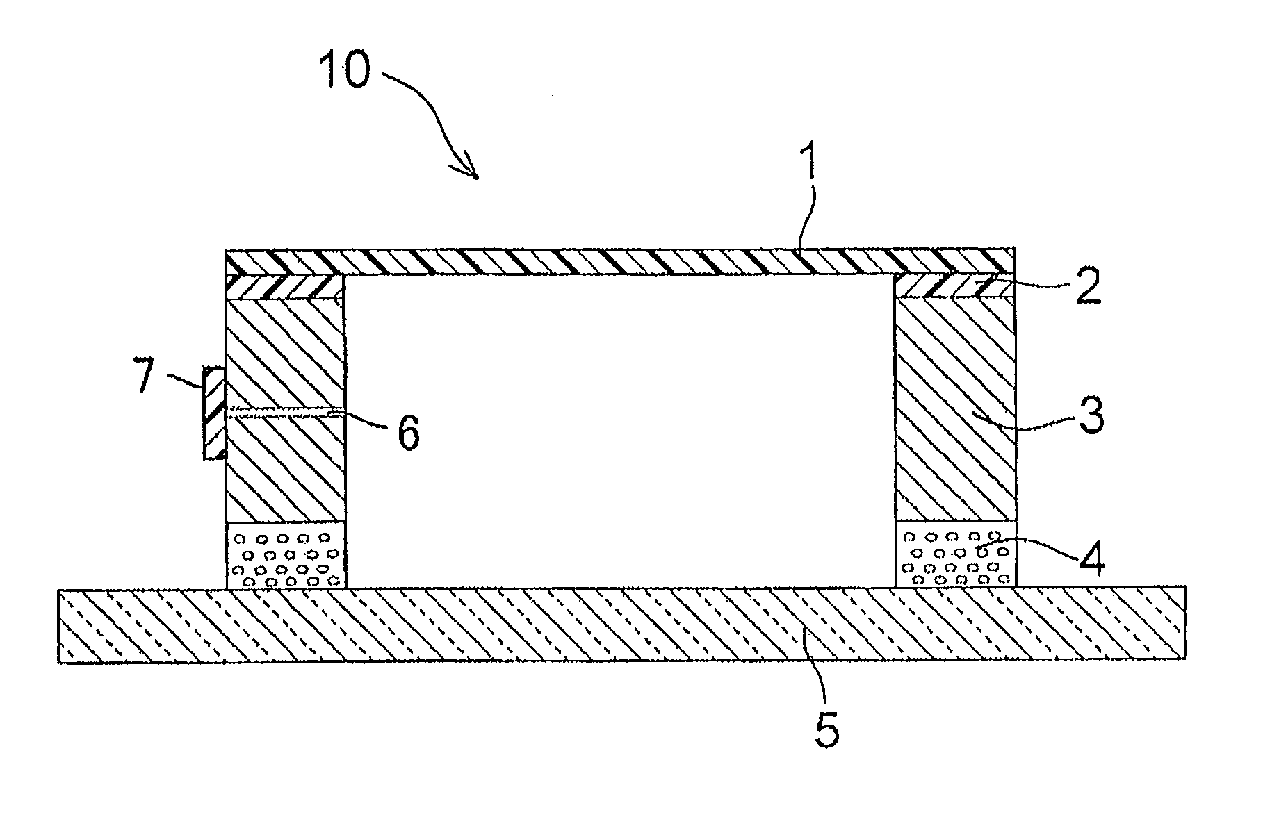
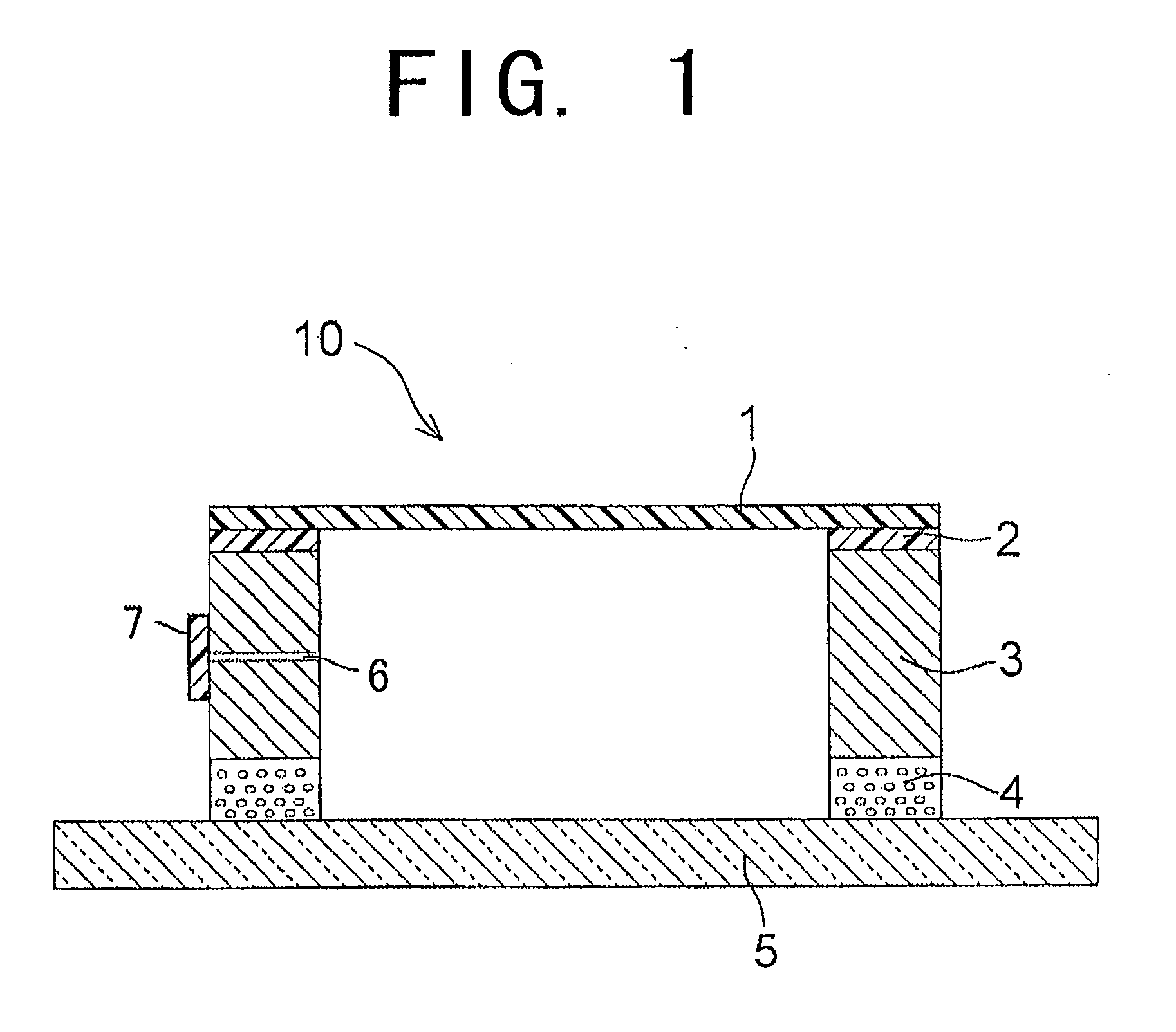
[0047]A pellicle frame made of an aluminum alloy having an outer size of 149 mm×113 mm×4.5 mm and a wall thickness of 2 mm was washed with deionized water and one surface of the pellicle frame was coated with a curable composition containing a straight chain perfluoro compound (Product Name “X-71-8023”) manufactured by Shin-Etsu Chemical Co., Ltd. to form an agglutinant layer. Immediately after forming the agglutinant layer, the pellicle frame was heated by electromagnetic induction to harden the curable composition contained in the agglutinant layer. The penetration of the hardened agglutinant layer as defined in ASTM D1403 was 100 and the thickness of the agglutinant layer was 0.3 mm.

[0048]On the other hand, the other surface of the pellicle frame opposite to the surface on which the agglutinant layer was formed was coated with a CYTOP adhesive agent (Product Name “CTX-A”) manufactured by ASAHI GLASS Co., Ltd. to form an adhesive layer. Then, the pellicle frame was heated at a tem...

working example 2

[0052]A pellicle frame made of an aluminum alloy, having an outer size of 149 mm×113 mm×4.5 mm and a wall thickness of 2 mm was washed with a deionized water and one surface of the pellicle frame was coated with a curable composition containing a straight chain perfluoro compound (Product Name “SIFEL8070”) manufactured by Shin-Etsu Chemical Co., Ltd. to form an agglutinant layer. A PET film was then brought into contact with the surface of the agglutinant layer. Thereafter, the pellicle frame was heated by electromagnetic induction to harden the curable composition contained in the agglutinant layer and the PET film was then peeled off the surface of the agglutinant layer. The penetration of the hardened agglutinant layer as defined in ASTM D1403 was 70 and the thickness of the agglutinant layer was 0.3 mm.

[0053]On the other hand, the other surface of the pellicle frame opposite to the surface on which the agglutinant layer was formed was coated with a CYTOP adhesive agent (Product ...

working example 3

[0057]A pellicle frame made of an aluminum alloy, having an outer size of 149 mm×113 mm×4.5 mm and a wall thickness of 2 mm was washed with a deionized water and one surface of the pellicle frame was coated with a curable composition containing a straight chain perfluoro compound (Product Name “X-71-8122”) manufactured by Shin-Etsu Chemical Co., Ltd. to form an agglutinant layer. A PET film was then brought into contact with the surface of the agglutinant layer. Thereafter, the pellicle frame was heated by electromagnetic induction to harden the curable composition contained in the agglutinant layer and the PET film was then peeled off from the surface of the agglutinant layer. The penetration of the hardened agglutinant layer as defined in ASTM D1403 was 70 and the thickness of the agglutinant layer was 0.3 mm.

[0058]On the other hand, the other surface of the pellicle frame opposite to the surface on which the agglutinant layer was formed was coated with a CYTOP adhesive agent (Pro...


PUM


Abstract

A pellicle 10 for lithography includes a pellicle frame 3, a pellicle membrane 1 adhered onto the upper end surface of the pellicle frame 3 and an agglutinant layer 4 formed on the lower surface of the pellicle frame 3 and the agglutinant layer 4 is formed by hardening a curable composition containing a straight chain perfluoro compound having a perfluoro structure in a main chain. The thus constituted pellicle 10 generates only a small amount of a decomposition gas even when it is used for a long time, thereby preventing solid-like foreign materials from separating out on a pattern region of a photomask 5 and can suppress degradation of an the agglutinant agent contained in an agglutinant layer 4 to be used for fixing a photomask 5 to the pellicle frame 3. Further, this pellicle 10 can be easily peeled off from a photomask 5 and replaced with a new one.

Description

BACKGROUND[0001]1. Technical Field[0002]The present invention relates to a pellicle for lithography for use as a dustproof cover for a photomask, a reticle or the like in the manufacture of a semiconductor device such as a large-scale integrated circuit, a very-large-scale integrated circuit (LSI) or the like or a liquid crystal display panel.[0003]2. Description of the Related Art[0004]In the case of manufacturing a semiconductor device such as a large-scale integrated circuit (LSI), a very-large-scale integrated circuit or the like, or a liquid crystal display panel, a semiconductor wafer or a mother substrate for a liquid crystal display panel is irradiated with exposure light via an exposure stencil such as a photomask or a reticle (hereinafter collectively referred to as “photomask” in this specification), whereby a pattern of the photomask is transferred onto the semiconductor wafer or the mother substrate for a liquid crystal display panel so that a pattern of the semiconduct...

Claims


Application Information

Patent Timeline
IPC IPC(8): G03F1/00G03F1/62H01L21/027
CPCG03F1/64G03F1/62G03F1/142G03F1/84
Inventor SHIRASAKI, TORUFUKUDA, KENICHI
Owner SHIN ETSU CHEM IND CO LTD
Why Eureka
Try Eureka