Apparatus and method for inspecting an object surface defect
- Summary
- Abstract
- Description
- Claims
- Application Information
AI Technical Summary
Benefits of technology
Problems solved by technology
Method used
Image

Examples
embodiment 1
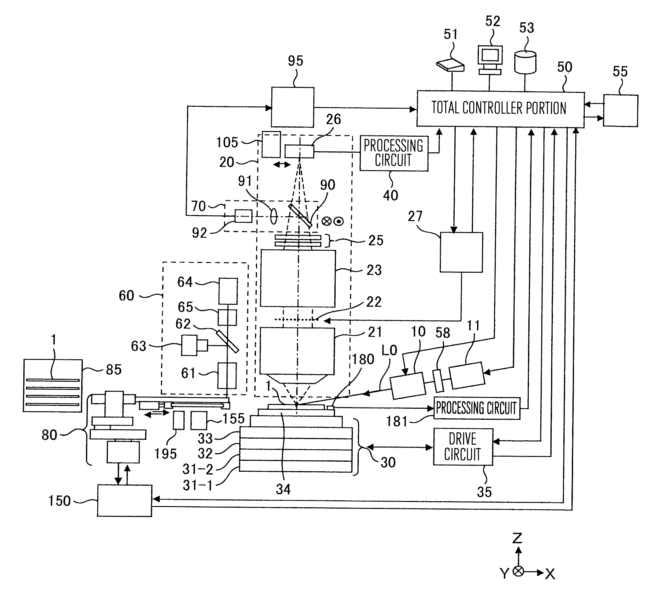
[0042]FIG. 1 shows a configuration of a defect inspection apparatus for an object surface according to a first embodiment. Broadly speaking, the present defect inspection apparatus includes an illumination optic system 10, a detection optic system 20, a conveyer system 30, a signal processing system 40, and a total controller portion 50 which controls the whole defect inspection apparatus.
[0043]The conveyer system 30 is configured to include, for example, an X stage 31-1, a Y stage 31-2, a Z stage 32, and a θ stage 33 for placing an inspection object substrate 1 such as a wafer, which is of various kinds and obtained from various manufacturing processes, on the mounting table 34 and for moving the substrate. The conveyer system 30 is configured to also include a drive circuit 35 for controlling those stages.
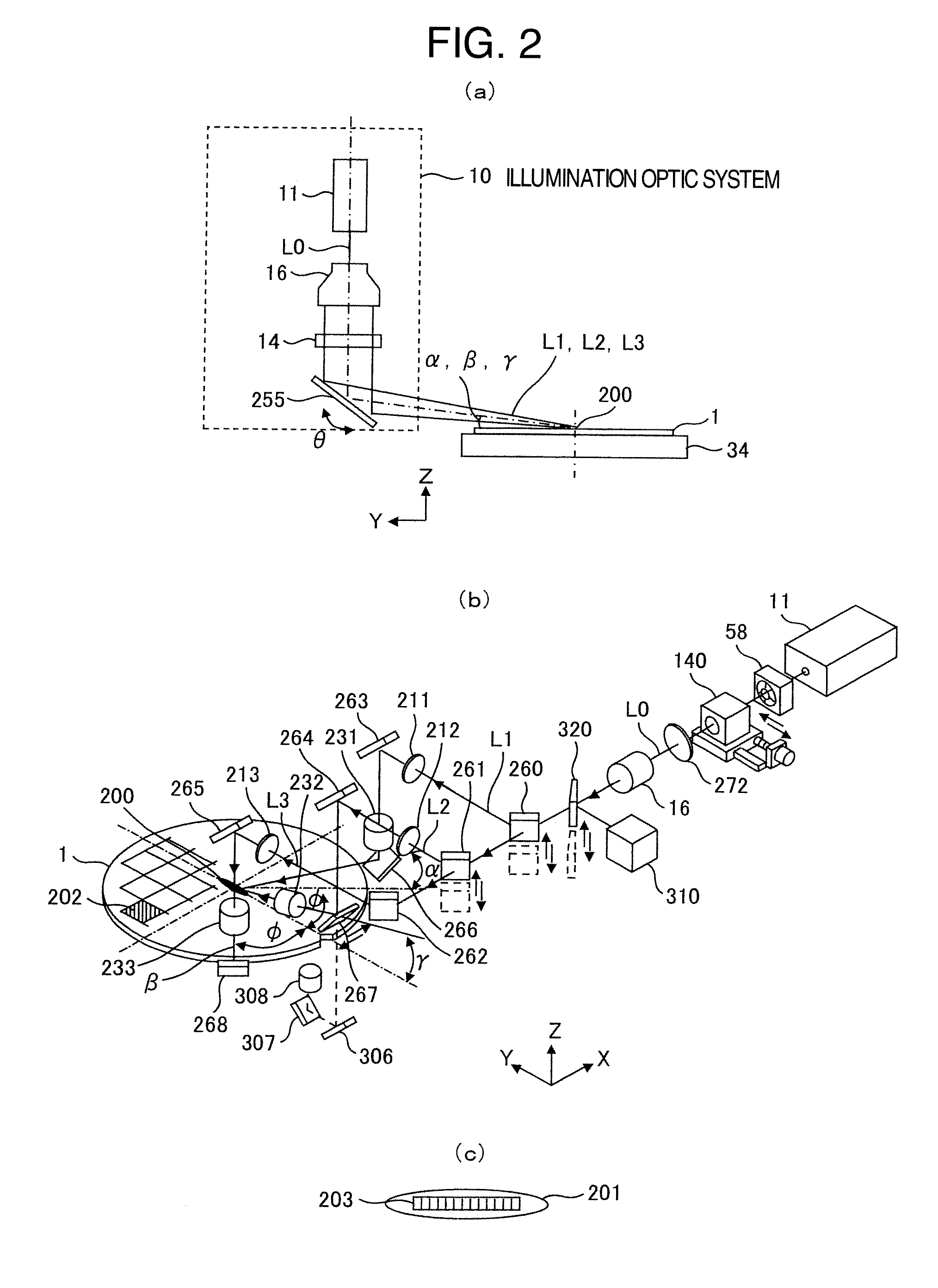
[0044]As shown in FIG. 2, the illumination optic system 10 includes, for example, a laser light source 11, a shutter 38, a beam expansion optic system 16, mirrors 260 to 268, len...
embodiment 2
[0069]Incidentally, for detecting minute defects on a highly integrated semiconductor substrate at a high speed, it is necessary to irradiate the top of the wafer 1 with a high luminance illumination beam and detect scattered light generated from a defect efficiently. Therefore, it is desirable that the irradiation region 201 of the slit-shaped beam 200 coincides on the wafer 1 with the pixel array of the photodetector 26 and the luminance distribution of the slit-shaped beam 200 takes, for example, a shape in line with the luminance distribution of the laser. During the inspection, an automatic focus system which is not described exercises control to provide the surface of the wafer 1 with a constant height with respect to an object focus of the detection optic system 20. Therefore, the irradiation region 201 of the slit-shaped beam 200 is maintained in a state in which it coincides on the wafer 1 with the pixel array of the photodetector 26. If the irradiation position of the illu...
embodiment 3
[0074]A method for detecting and correcting an anomaly of the detection optic system will now be described with reference to FIG. 12 and FIG. 13. The detection optic system 20 in the present defect inspection apparatus is a telecentric optic system formed of the object lens 21 and the imaging lens 23. For detecting defects stably in defect inspection, it is desirable that the performance of the detection optic system does not change from that at the time of manufacture. In the present invention, therefore, means for confirming the imaging performance of the detection optic system are provided on the way of the optical path and in the imaging position of the detection optic system.
[0075]In other words, as shown in FIG. 12, in a state in which a mirror 267 is saved in the Y direction, parallel laser light L0 emitted from the laser light source 11 is expanded by the beam expander 16, then a laser spot (point image) is formed in an object point position of the detection optic system 20 ...
PUM
 Abstract
Description
Claims
Application Information
 - Generate Ideas
- Intellectual Property
- Life Sciences
- Materials
- Tech Scout
- Unparalleled Data Quality
- Higher Quality Content
- 60% Fewer Hallucinations
Browse by: Latest US Patents, China's latest patents, Technical Efficacy Thesaurus, Application Domain, Technology Topic, Popular Technical Reports.
© 2025 PatSnap. All rights reserved.Legal|Privacy policy|Modern Slavery Act Transparency Statement|Sitemap|About US| Contact US: help@patsnap.com