Solderless back contact solar cell module assembly process

a solar cell and module technology, applied in the direction of photovoltaics, electrical equipment, semiconductor devices, etc., can solve the problems of metallization, difficult to handle without fracture, and large cost of silicon itself, and achieve the effect of less handling of fragile wafers

Inactive Publication Date: 2011-06-23
HIESLMAIR HENRY
View PDF9 Cites 29 Cited by
  • Summary
  • Abstract
  • Description
  • Claims
  • Application Information

AI Technical Summary

Benefits of technology

[0016]In one embodiment, the back contact silicon cells, bypass diodes and external leads are first laminated to the front module glass (leaving the backside of the cell exposed). This provides needed mechanical support when using thin silicon wafers. The full metallization is performed by electro or electroless plating of the entire module, eliminating any need for soldering.

Problems solved by technology

In solar cells based on crystalline silicon, the silicon itself is a major cost.
A 100 um silicon wafer is very fragile and difficult to handle without fracture.
Metallization is an ongoing issue with solar cells.
Because screen printing and firing of metal pastes produces poor results, many alternative approaches have been pursued.
Some can be quite complex and require many steps and alignments.
Process complexity is at odds with low cost.
While such solar cells are common, they have the drawback that the metal collection fingers on the front side shade portions of the solar cell, thereby causing efficiency losses.
In order to electrically connect cells in series, conductors need to be soldered to the front side of one cell and then soldered to the back side of the next cell, increasing the handling and assembly complexity.
A disadvantage of the back contact cell design which has hindered more wide spread adoption, is that the metal on the backside must be patterned such that the two polarities are electrically isolated from each other.
This larger area, unfortunately, reduces the usable area of the wafer by not allowing collection fingers of the opposite polarity into the areas of the bond pads.
Additionally, the metal pattern must have low resistance which usually results in thicker metal layers.
However, the fingers themselves must be of low resistance.
This has been difficult to accomplish with few process steps and inexpensively.
This has a number of processing steps as well as inherent limits on the minimal distances between the

Method used


Image

  • Solderless back contact solar cell module assembly process
  • Solderless back contact solar cell module assembly process
  • Solderless back contact solar cell module assembly process

Examples


Embodiment Construction

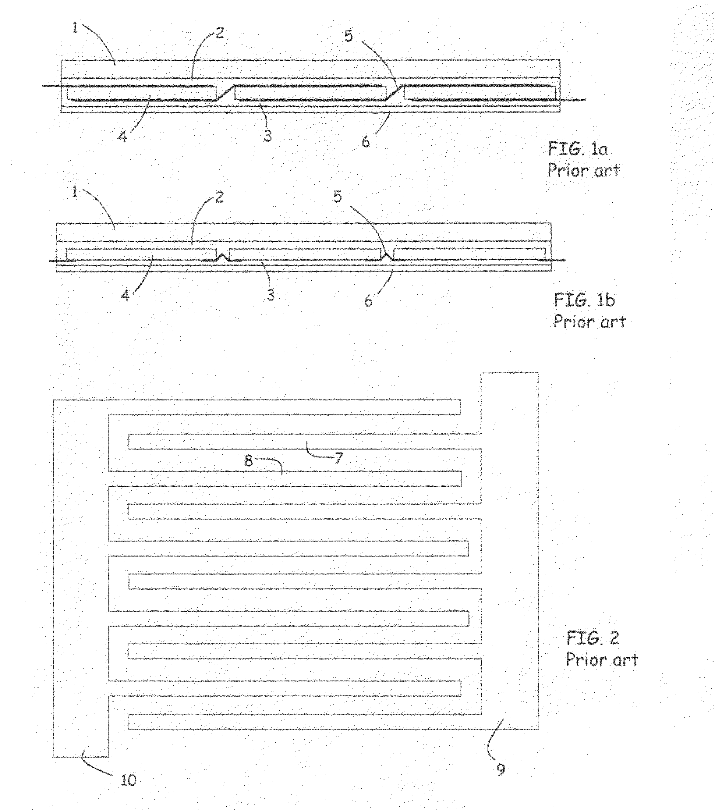
[0029]This invention relates to processing of thin back contact solar cell wafers into modules. The wafers should already have appropriately doped regions. Since the metal is being plated, a seed metal pattern is required. The thickness of the seed layer can be from 0.1 microns to 100 microns. The formation of the seed metal pattern can be done before or after the wafer is laminated to the front glass of the module.

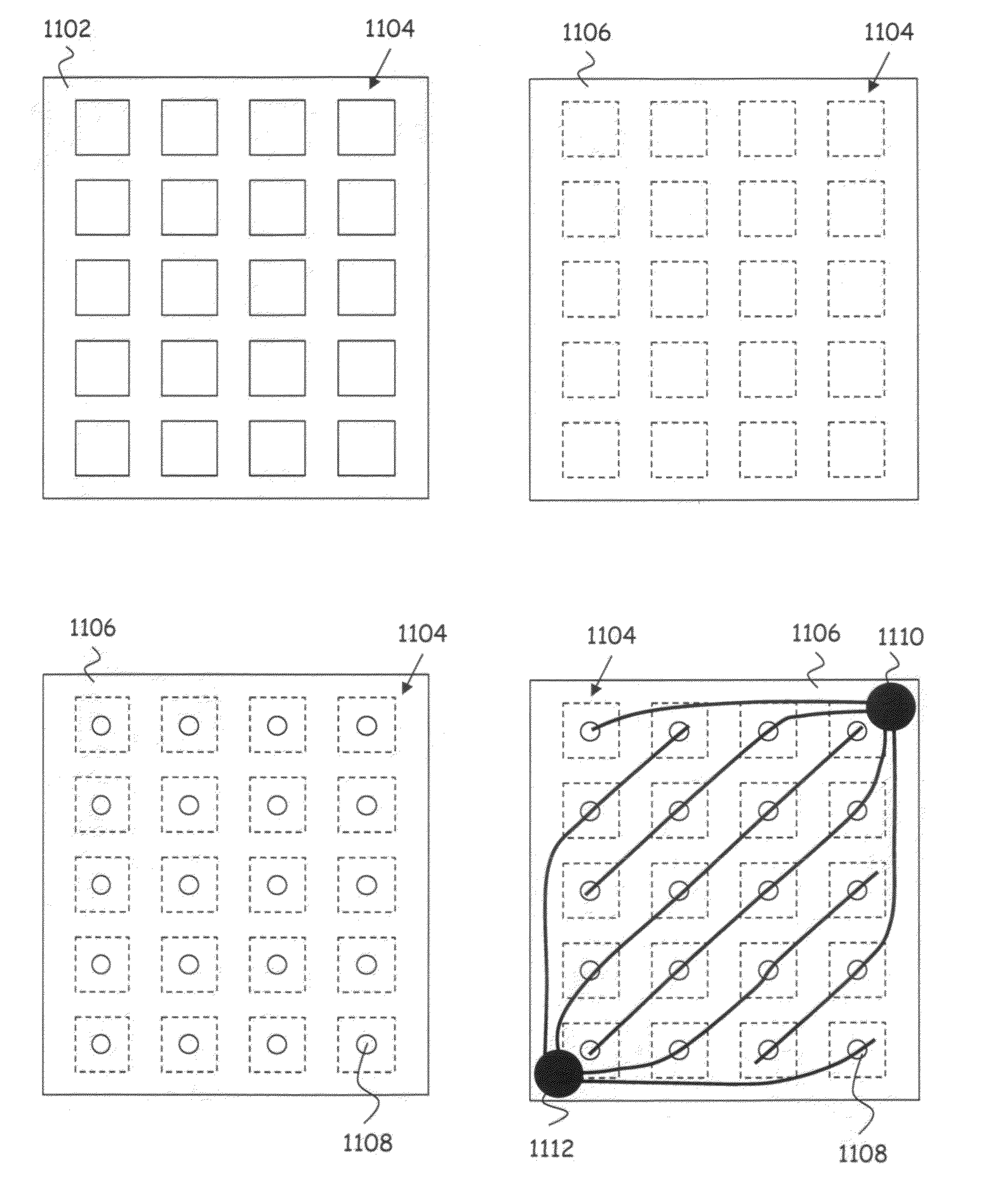
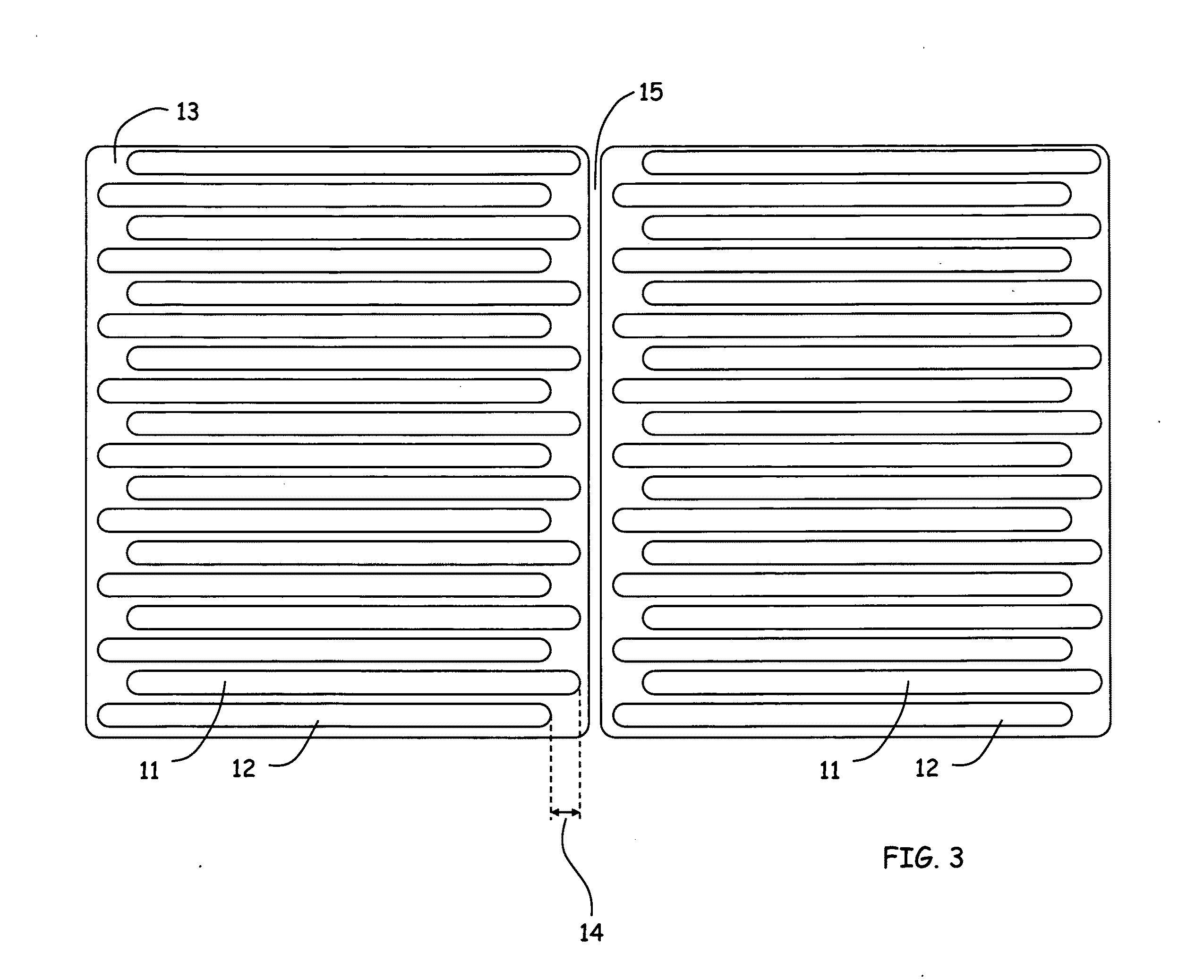
[0030]While a regular interdigitated contact structure can be used, the preferred thin seed metal pattern is that of slightly shifted stripes 11, 12 as in FIG. 3. Here 15 is the seam between adjacent solar cells. Stripes of one polarity are shifted toward one edge and the other polarity toward the other edge. The amount of shifting 14 is preferably greater than 0.1 mm and less than 8 mm. The shifting makes it easier for simple printing to contact alternate stripes. The stripes, however, need not be shifted. Some printing techniques have high enough resolution, such as ink...


PUM


Abstract

In order to better and more efficiently assemble back contact solar cells into modules, the cell to cell soldering and other soldered connections are replaced by electro and/or electroless plating. Back contact solar cells, diodes and external leads can be first laminated to the module front glass for support and stability. Conductive materials are deposited selectively to create a plating seed pattern for the entire module circuit. Subsequent plating steps create an integrated cell and module metallization. This avoids stringing and tabbing and the associated soldering steps. This process is easier for mass manufacturing and is advantageous for handling fragile silicon solar cells. Additionally, since highly corrosion resistant metals can be plated, the moisture barrier requirements of the back side materials can be greatly relaxed. This can simplify and reduce the cost of the back side of the module.

Description

CROSS REFERENCE TO RELATED APPLICATIONS[0001]This application claims the benefit of U.S. provisional patent application 61 / 284,584, filed on Dec. 22, 2009, entitled “Solderless Back Contact Solar Cell Module Assembly Process”, and hereby incorporated by reference in its entirety.FIELD OF INVENTION[0002]The invention relates to a back contact solar cell metallization and module assembly process. In particular this disclosure relates to metal plating on the cell and module level for efficient assembly and connection.BACKGROUND[0003]Photovoltaic solar cells are semiconductor devices that convert light energy to useful electrical energy. Generally speaking, a solar cell typically includes a silicon wafer having regions of n-type doping and regions of p-type doping. Solar radiation generates mobile electrons and holes that migrate to the different regions and create a voltage differential between the two regions. Patterned metal layers on the silicon wafer are required to conduct the gen...

Claims


Application Information

Patent Timeline
IPC IPC(8): H01L31/05H01L31/18
CPCH01L31/048H01L31/0516H01L31/0512Y02E10/50
Inventor HIESLMAIR, HENRY
Owner HIESLMAIR HENRY
Why Eureka
Try Eureka