Integrated circuit

a technology of integrated circuits and circuits, applied in pulse manipulation, pulse techniques, instruments, etc., can solve the problems of reproducibility and supply rejection, inability to meet the requirements of process specifications or process capabilities, and inability to meet the requirements of accuracy, etc., to achieve the effect of increasing parametric accuracy, increasing yield and increasing accuracy

Active Publication Date: 2011-08-04
NXP BV
View PDF11 Cites 2 Cited by
  • Summary
  • Abstract
  • Description
  • Claims
  • Application Information

AI Technical Summary

Benefits of technology

[0010]The principles of the invention are advantageous as the yield can be increased due to an increased parametric accuracy and cost related to upgrading manufacturing equipment for the sole reason of increased accuracy can be avoided. Different versions can be consolidated into a single product that is tailored in the final stages of production by trimming the circuits thus simplifying the supply chain, and reducing the qualification effort. Electrical trimming of circuits can be performed at final test to correct inaccuracies in packaging and all prior manufacturing. Most other trimming methods require physical access to the silicon die. The trimming is reversible to allow re-calibration or adjustments in the field and adaptation to unanticipated new applications of the product. The product can even be trimmed after the packaged die is mounted on the circuit board. Many-time-programmable cells MTP are non-destructive; and the material integrity is maintained over large number of read / write cycles. Destructive methods introduce inherent uncertainty with respect to the product quality and reliability. Reverse engineering is much more difficult on MTP than physical trimmings. This makes the MTP product more resistant to copying or tampering. Non-volatile trimming is completely transparent to the end user; no special interface or procedure is required after final test. Once programmed, no more power is needed to sustain the calibrated state, this is an advantage over conventional varactor-based approach where a supply voltage is needed and inevitably power is dissipated and susceptibility to cross-talk is increased. The variable component is not connected to a power supply, hence it inherently has a very high supply rejection. Here, the MTP concept is used in a switch that connects analog elements e.g. in a high-frequency circuit.
[0011]It should be noted that according to ht invention existing features that can be found in CMOS, power management and BiCMOS technologies are used such that no specific manufacturing requirement are present. The non-volatile functionality is added without increasing the manufacturing complexity.

Problems solved by technology

In some cases the accuracy requirements may exceed the process specifications or process capability.
All of these implementations however must rely on active circuitry (e.g. an accurate voltage source connected to a variable capacitor) that in-turn may only have a limited accuracy, reproducibility and supply-rejection.
However, all of these techniques are expensive due to the fact that they require specialized equipment and a complex mix of fabrication steps (the physical trimming process) and verification steps (electrical measurements).
Moreover, they require a physical access to the die which makes a trimming after packaging rather difficult.

Method used


Image

  • Integrated circuit
  • Integrated circuit
  • Integrated circuit

Examples


first embodiment

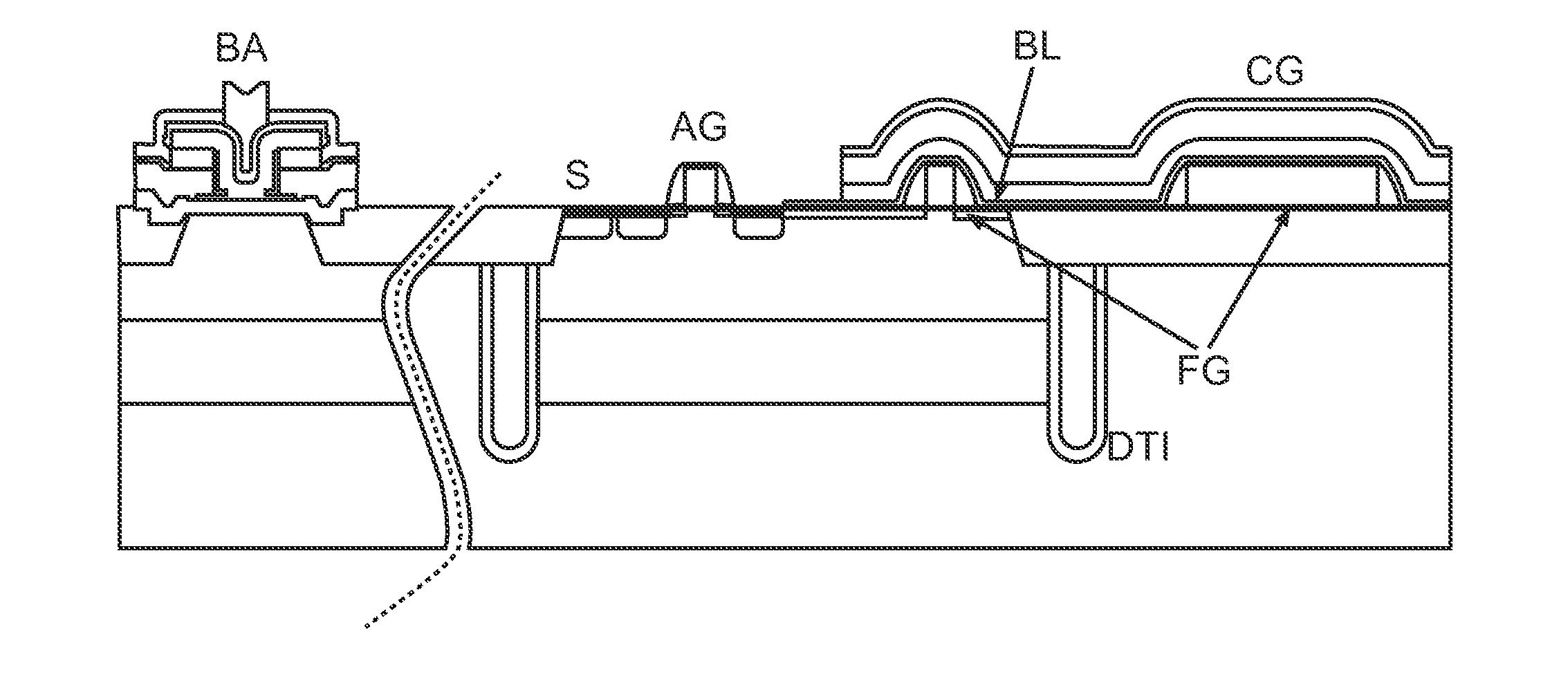
[0021]FIG. 1 shows a schematic cross section of part of an integrated circuit according to a Here, a many-times-programmable cell having a MOS transistor with a floating gate FG is depicted. The cell can comprises a source S, an access gate AG, a bil line BL and a control gate CG. The floating gate FG may comprise a tunnel oxide TO and is connected to a first low-leakage capacitor that may have a tunnel oxide TO as its dielectric material. However, it should be noted that any other low-leakage capacitor that is substantially larger than the gate-channel capacitance of the MOS and that has sufficient breakdown be sufficient.

[0022]It should be noted that an operation of many-time-programmable cells MTP is very similar to conventional non-volatile memory while the process complexity is much lower (only a single gate-poly is required) and the memory cell is bigger in size. Instead of retaining digital bits, the cell MTP is used according to the invention as a (semi-permanent) switch to...

second embodiment

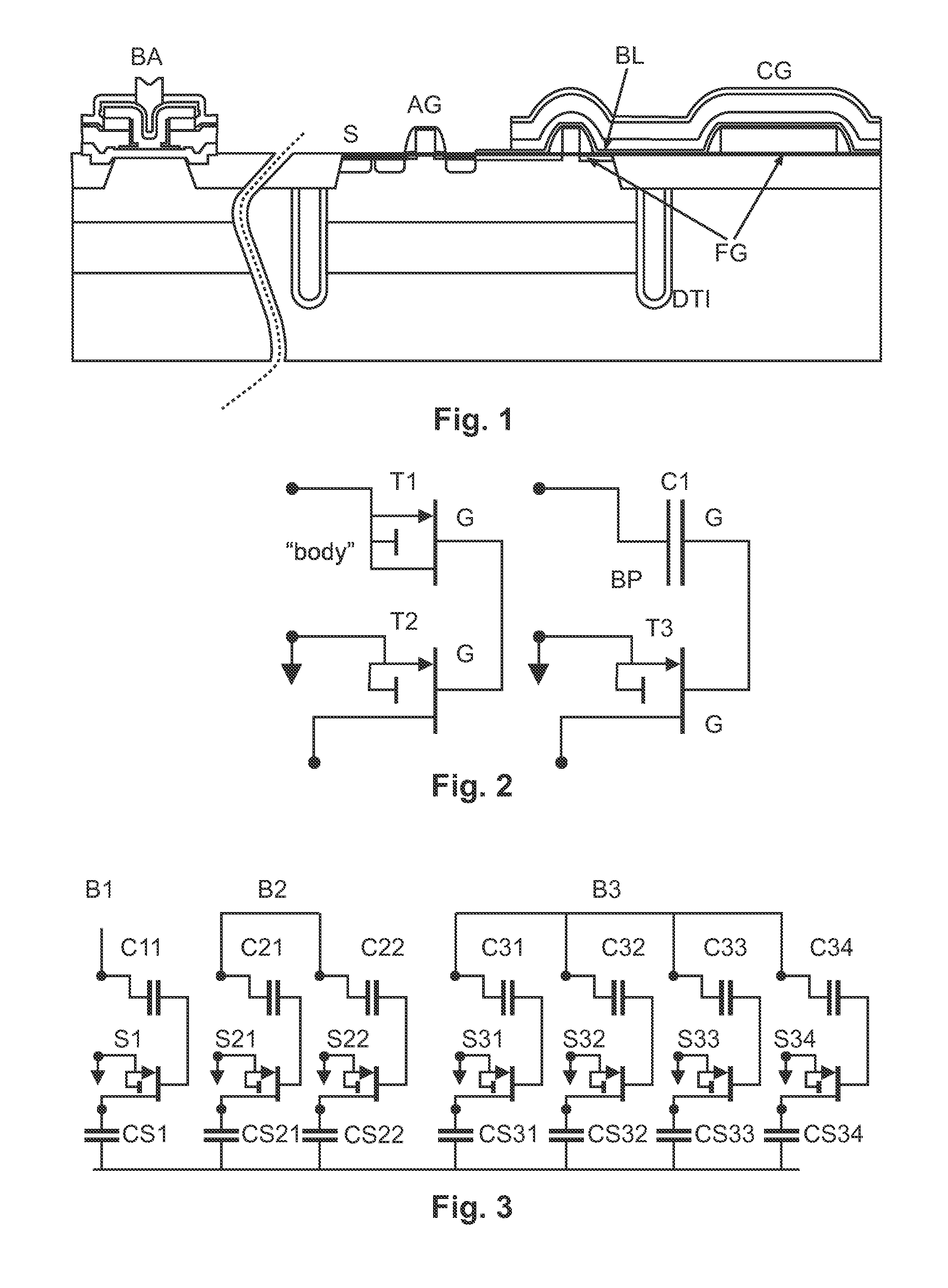
[0027]FIG. 2 shows a circuit diagram of a switching unit according to a On the left the conceptual CMOS implementation, and on the right a BiCMOS implementation is depicted. The CMOS implementation comprises a first and second transistor, wherein the gates G of the first and second transistor are coupled together. The source and drain of the first transistor are coupled together with the body terminal. The first transistor is implemented as the floating gate. The BiCMOS implementation enables a forming of the capacitor to the floating gate. Hence, the capacitor C1 is implemented between the gate G of the transistor T3 and a base poly BP. To enable a retention of charge the floating gate should be without contacts or any connection to interconnect. Therefore, capacitive coupling to the gate must be achieved with a layer in close proximity. In a CMOS implementation this can be achieved through a MOS gate as depicted on the left side of FIG. 2. A BiCMOS implementation enables some add...

third embodiment

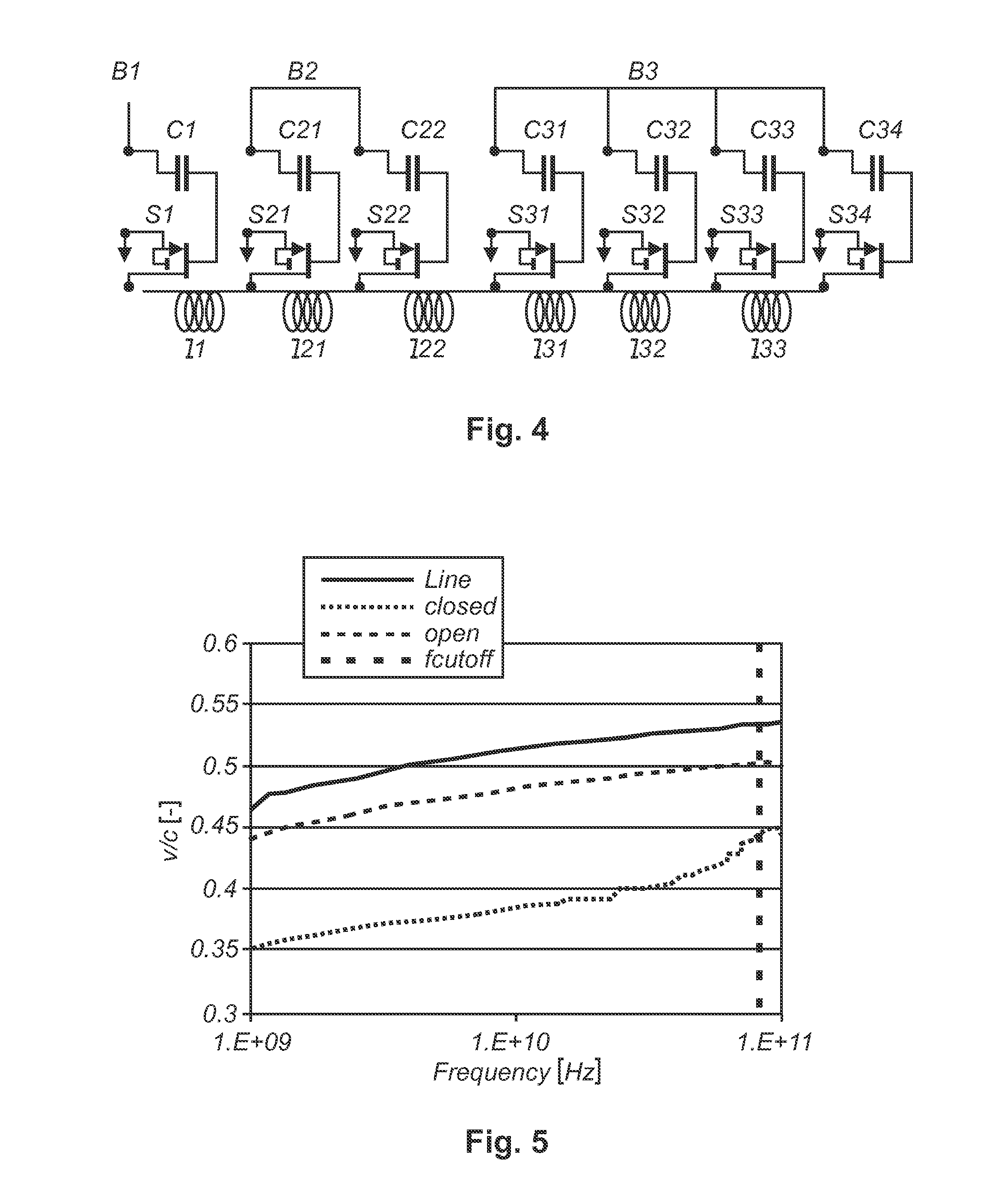
[0050]FIG. 4 shows a circuit diagram of a trimming unit and an inductor unit according to a Here, a trimmable series inductor is depicted. Switches or switching units are grouped in “bits” where the nth bit B1-B3 contains 2n switches S1; S21, S22; S31, S32, S33; S34, wherein each switch is coupled to a first capacitor C11, C21, C22, C31, C32, C33, C34, respectively. Each switching group is coupled to an inductor element, i.e. the switching group B1 is coupled to an inductor element I1, the switching group B2 is coupled to two inductor elements I21, I22 while the switching group B3 is coupled to the inductor elements I31, I32, I33, I34. In other words the numbers of inductor elements correspond to the number of switches.

[0051]Hence, the switching units can be used for connecting an inductive component in series. The drain capacitance of the switching units can lead to a resonance thus limiting the maximum operating frequency for a given resistance in the closed state. To achieve par...


PUM


Abstract

An integrated circuit is provided, which comprises at least one first group each having at least one analog unit; and at least one second group each having at least one electronically settable semi-permanent switching unit coupled to the at least analog unit of the first group for trimming the first group and having at least one many-times-programmable and non-volatile cell (MTP). Each many-times-programmable cell (MTP) comprises at least one MOS transistor having a floating gate (FG) with a tunnel oxide (TO) and a first capacitor coupled to the floating gate (FG). The capacitance of the first capacitor is substantially larger than a gate-channel capacitance of the MOS transistor.

Description

FIELD OF THE INVENTION[0001]The present invention relates to an integrated circuit.BACKGROUND OF THE INVENTION[0002]In the area of application-specific analog integrated circuits a tight control of the parameters of the IC manufacturing process maybe required. In some cases the accuracy requirements may exceed the process specifications or process capability. One way to deal with these problems is to implement some form of flexibility in the circuitry. A well-known example is the voltage-controlled oscillator. Here, a variable capacitor is used to enable a small variation in the oscillation frequency due to a variation in the control voltage. Similar principles can be applied to all other analog components such as filters, impedance matching networks amplifiers and the like.[0003]All of these implementations however must rely on active circuitry (e.g. an accurate voltage source connected to a variable capacitor) that in-turn may only have a limited accuracy, reproducibility and supp...

Claims


Application Information

Patent Timeline
Patent Type & Authority Applications(United States)
IPC IPC(8): H01L27/105B82Y99/00
CPCG11C16/0416G11C27/005G11C2216/10H01L21/8249H01L27/1026H03M1/802H01L27/115H01L27/11517H01L29/792H03K5/133H03K2005/00019H01L27/105H10B69/00H10B41/00
Inventor VAN NOORT, WIBO D.LETAVIC, THEODORE J.ZAATO, FRANCIS
Owner NXP BV
Why Eureka
Try Eureka