
Method for connecting thin-film solar cells and thin-film solar module

a solar cell and solar module technology, applied in the direction of photovoltaic energy generation, pressure inorganic powder coating, photovoltaic energy generation, etc., can solve the problems of not all materials can be soldered conventionally, increase assembly expenditure, and unsatisfactory resistance of adhesive to moisture and higher temperatures, so as to reduce manufacturing costs, avoid short circuits, and simplify manufacturing processes

Inactive Publication Date: 2011-08-18
MALIBU
View PDF7 Cites 4 Cited by
  • Summary
  • Abstract
  • Description
  • Claims
  • Application Information

AI Technical Summary

Benefits of technology

[0007]The current collecting paths and the optionally provided current paths usually consist of tin-plated copper strips. It is known to adhesively bond these strips to the semiconductor layers by an electrically conductive adhesive. The known adhesives used for this purpose, for example, have a plurality of disadvantages such as an unsatisfactory resistance of the adhesive to moisture and higher temperatures. The contamination of individual cells by components of the adhesive should be assessed equally critically. In addition, the relatively complex mechanical and thermal process control during application of the adhesive increases the assembly expenditure.
[0046]According to another embodiment of the present disclosure, the current paths without insulating film are not formed at the edge of the support material but further towards the center of the module. In this case it is necessary that the individual solar cells or the entire module separate the region of the active cells from that of the current path by way of an insulation structure which extends as far as onto the glass substrate or superstrate, for example, by laser ablation or mechanical scoring, in order to avoid a short circuit. In order to improve the metal adhesion on the substrate or superstrate, the fields for the current paths can be provided with additional insulation structures, such as scoring the deposited layer. In addition, further insulation structures can be attached for better adhesion of the current collecting paths.

Problems solved by technology

The known adhesives used for this purpose, for example, have a plurality of disadvantages such as an unsatisfactory resistance of the adhesive to moisture and higher temperatures.
In addition, the relatively complex mechanical and thermal process control during application of the adhesive increases the assembly expenditure.
A problem here is that not all materials can be soldered conventionally, for example, ceramic, TCO, or transparent conductive oxide such as, for example, ZnO, SnO2, ITO or aluminium.
Furthermore, local mechanical stresses caused by spot soldering are disadvantageous.
A disadvantage here, however, is that a very expensive special solder is required for the ultrasound soldering of metal strips to TCO.
The relatively complex mechanical process control and the difficult process monitoring also have a negative effect.
As a result of the high temperatures, for example, see column 4, lines 6 and 7 of the '645 document, the methods are not suitable for applying conductor paths to thin-film solar cells because, for example, the severely heated particles oxdize upon contact with oxygen.
In the case of a glass support, the thermal loading can also lead to its fracture.
The carrier gas heated to several hundred degrees expands in the nozzle and brings about the necessary high velocities of the particles.
By this method, very complex contacting patterns can be produced on the solar module.
The electrical contacting of the copper strips with the solar cells is, however, no longer accomplished with conducting adhesives but by sprayed-on metal in the cold gas spraying process.

Method used


Image

  • Method for connecting thin-film solar cells and thin-film solar module
  • Method for connecting thin-film solar cells and thin-film solar module
  • Method for connecting thin-film solar cells and thin-film solar module

Examples


Embodiment Construction

the substrate approach, optical transparency of the support material can be dispensed with since the support is located in the beam path after the functional layers.

[0053]Instead of only one junction box, it is within the scope of the present disclosure to use two such boxes. Then, no current paths are required.

BRIEF DESCRIPTION OF THE DRAWINGS

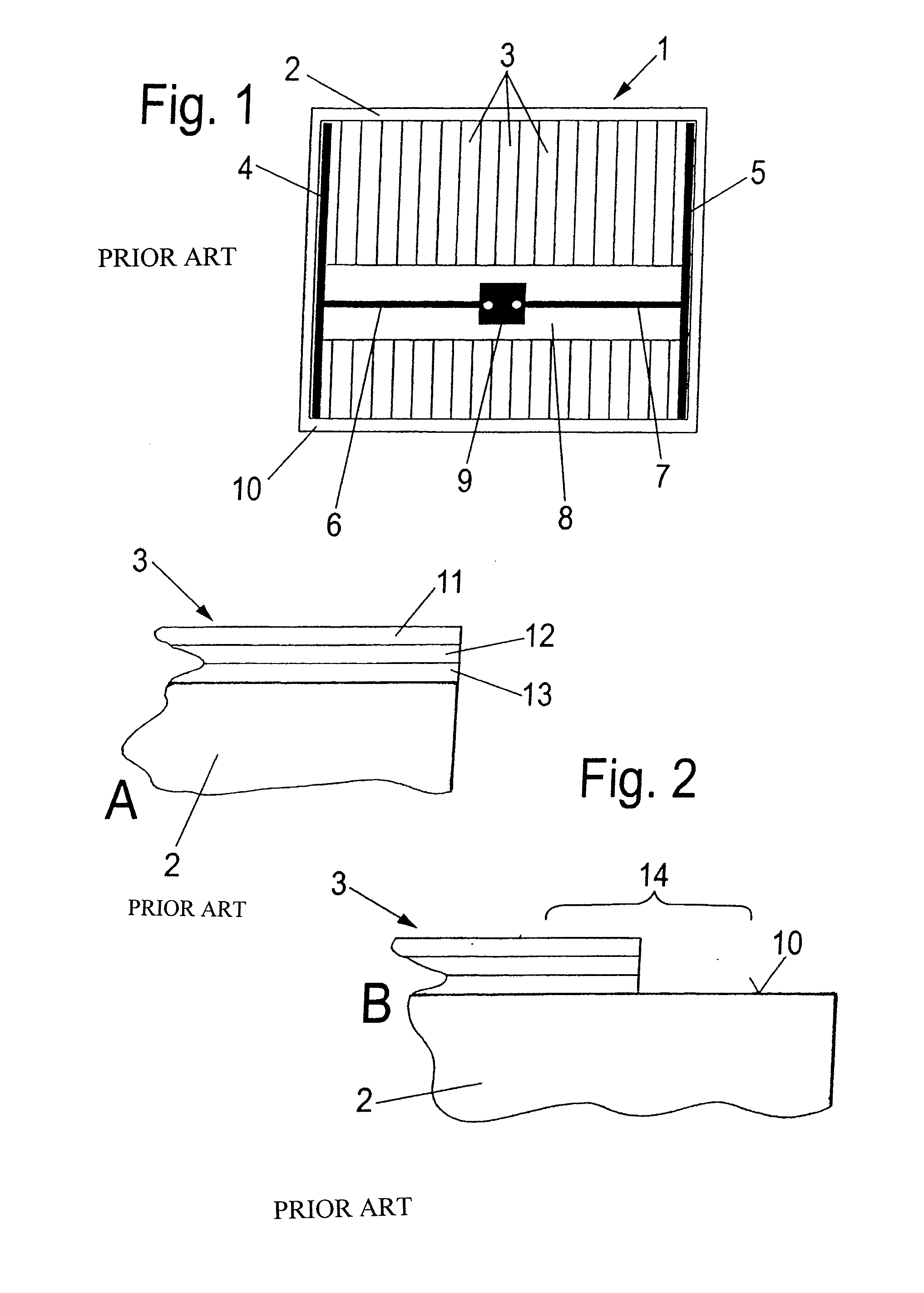
[0054]FIG. 1 shows a plan view of a known thin-film solar module.

[0055]FIGS. 2A and 2B show a known thin-film solar cell in cutaway and enlarged view in an edge region.

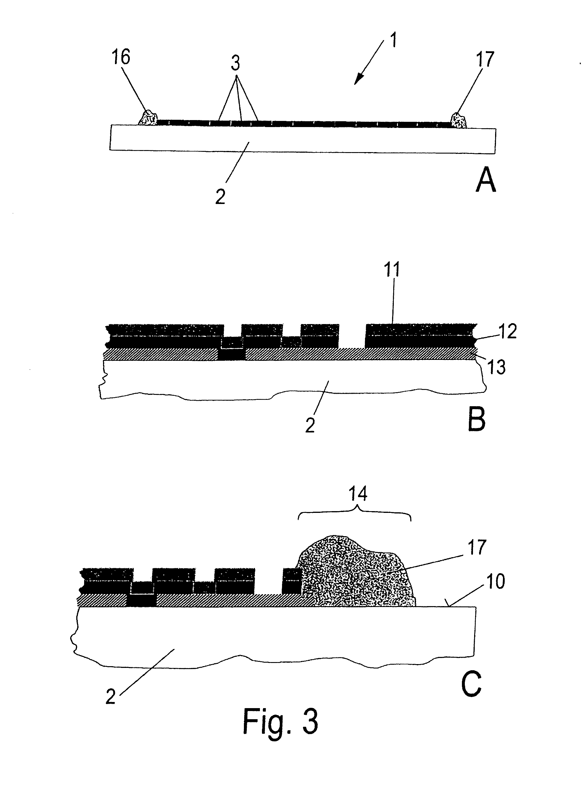
[0056]FIG. 3A shows a schematic sectional view of a thin-film solar module provided with cold-gas sprayed current collecting paths, according to the present disclosure.

[0057]FIG. 3B shows a sectional view of a thin-film solar module in a known state of process before a cold gas spraying step shown in FIG. 3C according to the present disclosure.

[0058]FIG. 3C shows a sectional view of an edge region of a thin-film solar module provided with a cold-gas sprayed current collecting pa...


PUM

PropertyMeasurementUnit
Grain sizeaaaaaaaaaa
Temperatureaaaaaaaaaa

Abstract

A method for forming at least one electrically conducting contact area on a thin-film solar module. The method steps include providing a plurality of thin-film solar cells including cell material layers; applying the thin-film solar cells to a support material; and forming the at least one electrically conducting contact area on the thin-film solar module by using a cold gas spraying process. A thin-film solar module includes a support material, a plurality of cell material layers applied to the support material, and at least one electrically conducting contact area formed on the thin-film solar module by a cold gas spraying process.

Description

[0001]This application is a national stage of International Application PCT / EP2009 / 061932, filed Sep. 15, 2009, and claims benefit of and priority to German Patent Application No. 10 2008 051 469.1, filed Oct. 13, 2008, the content of which Applications are incorporated by reference herein.BACKGROUND AND SUMMARY[0002]The present disclosure relates to a method for forming at least one electrically conducting contact area on a thin-film solar module. The method steps include providing a plurality of thin-film solar cells including cell material layers and applying the thin-film solar cells to a support material. The present disclosure also relates to a solar module formed by the above-noted method.[0003]A thin-film solar module, as noted above, comprises a plurality of solar cells arranged on a support material, such as a substrate or superstrate, which may be a glass panel. Each generate current according to the principle of a photodiode, where electron-hole pairs are generated by in...

Claims


Application Information

Patent Timeline
IPC IPC(8): H01L31/05H01L31/0224
CPCC23C24/04H02S40/34Y02E10/50H01L31/022425
Inventor PFEUFFER, ALEXANDER
Owner MALIBU
Learn More