Chalcogenide-based materials and improved methods of making such materials

a technology of chalcogenide-based materials and photoabsorbing materials, which is applied in the direction of sustainable manufacturing/processing, camera filters, instruments, etc., can solve the problems of stoichiometry, stoichiometry, and inability to meet the requirements of photoabsorbing compositions with industrially scalable processes, and achieves the reduction of overall void area and size, improve adhesion, and reduce the effect of ga migration

Inactive Publication Date: 2011-09-22
DOW GLOBAL TECH LLC
View PDF23 Cites 24 Cited by
  • Summary
  • Abstract
  • Description
  • Claims
  • Application Information

AI Technical Summary

Benefits of technology

[0013]The present invention provides strategies for making high quality CIGS photoabsorbing compositions from sputtered precursor film(s) that incorporate chalcogen(s) with a sub-stoichiometric concentration, with the option of localizing a sub-layer of this chalcogen-containing layer at a specific location within the precursor film(s). The conversion of these precursors into CIGS photoabsorbing material via a following chalcogenizing treatment (also referred to as “post-chalcogenization,” including, e.g., “post-selenization” when Se is used) provides one or more or all of the f

Problems solved by technology

Crystalline silicon-based absorbers tend to be rigid, not flexible.
Making stoichiometric, photoabsorbing compositions with industrially scalable processes, however, continues to be quite challenging.
There are many serious challenges to overcome with this approach.
As one challenge, chalcogenizing a precursor tends to induce significant volume expansion of the film.
This expansion can cause mechanical stresses that reduce adhesion, induce stresses, and/or other problems.
Additionally, very large voids tend to form in large part at the bottom of the film adjacent the backside contact (e.g., a Mo layer in many instances) as a consequence of chalcogenizing the precursor.
These large voids tend to cause adhesion problems between the CIGS layer and the backside contact layer.
Electronic performance and service life also can be seriously compromised.
These large voids also can induce mechanical stresses that lead to delamination, fractures, and the like.
As another drawback, post-selenization processes tend to induce significant gallium migration in the film.
The top of the film may become completely Ga depleted.
This may have negative repercussions for film adhesion.
Even more importantly, if some Ga is not located within the region of th

Method used


Image

  • Chalcogenide-based materials and improved methods of making such materials
  • Chalcogenide-based materials and improved methods of making such materials
  • Chalcogenide-based materials and improved methods of making such materials

Examples


example 1

Preparation of CIGS Film Embodiment of the Present Invention

[0100]A CIGS film precursor is produced with a relatively high but sub stoichiometric level of Se throughout the precursor film. A “CIGS” sputter target (commercially available) containing the atomic ratios of In+Ga / Cu of 1.2, Ga / In of 0.3, and Se / (Cu+In+Ga)=2, 2″ in diameter, is used to sputter the precursor film. The method used is pulsed DC (direct current) sputtering, with a pulse frequency of 330 kHz and an off time of 1.2 vs. The substrate is located 8 cm away from the target. The substrate is a piece of soda-lime glass coated with a 800 nm thick layer of Mo. The substrate was not intentionally heated during sputtering, but the substrate temperature during growth is estimated to be approximately 60° C. throughout the growth of the precursor film. The base pressure of the system is under 5*10−7 Torr; the sputtering pressure is 3.5 mTorr using ultra high purity Argon gas. The target is sputtered at a power of 100 W for ...

example 2

Preparation of CIGS Film Embodiment of the Present Invention

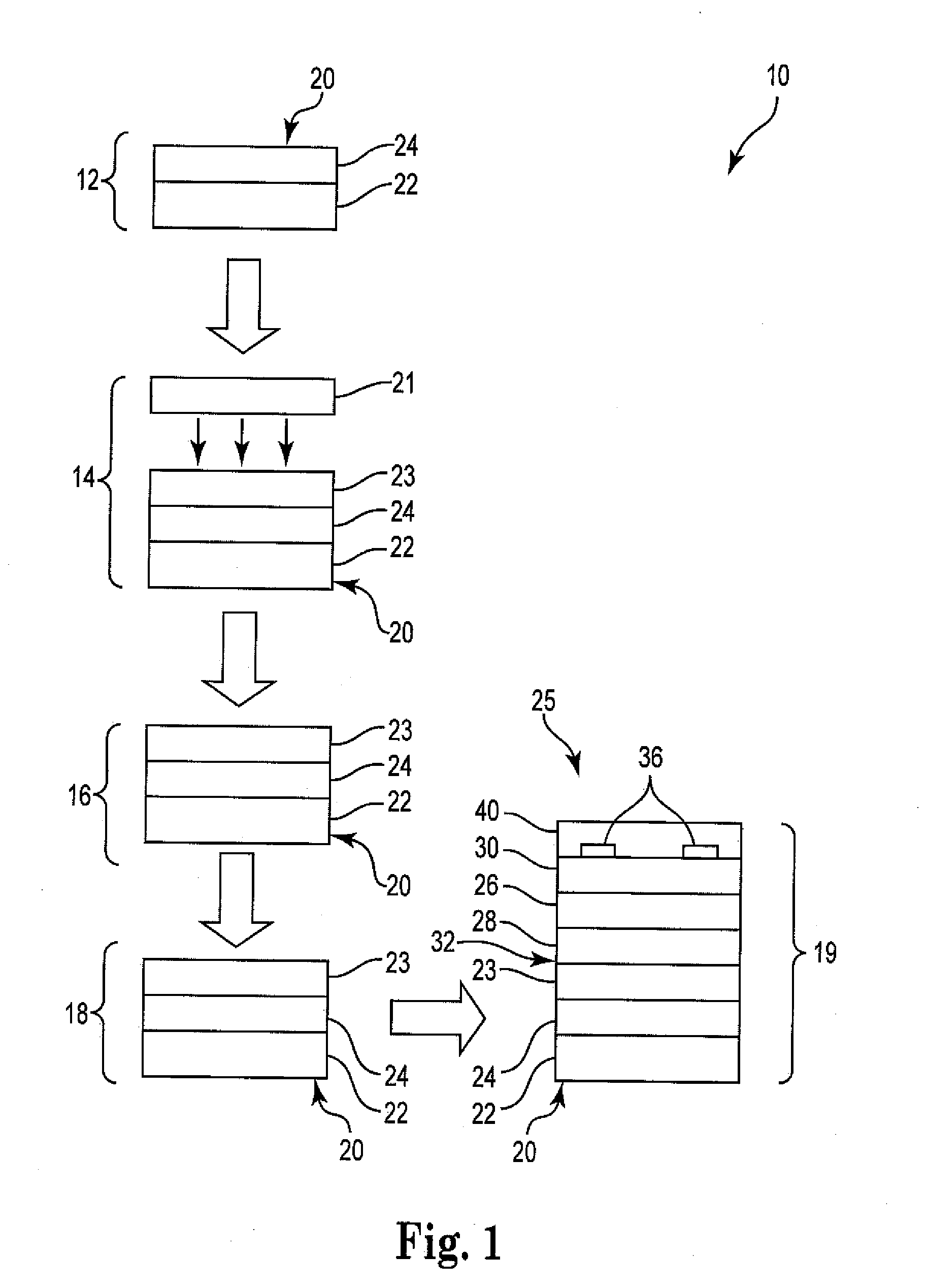
[0103]A CIGS film precursor is prepared with a relatively low, substoichiometric level of Se throughout the film. This film precursor is deposited with both a CIGS alloy target (Cu, In, Ga, and Se included in the target) similar to the one used in Example 1 except that the diameter is 100 mm, and a CIG alloy target (Cu and In and Ga included in the target) similar to the one used for comparative example A. The two targets are sputtered at the same time in a confocal arrangement, both at 100 W for 30 minutes at room temperature. As the CIGS target sputters much more slowly than the CIG target, this results in a bulk film with a relatively low concentration of Se throughout. In this case, the targets were 100 nm in diameter, and the substrate is a 5×5″ piece of stainless steel coated with Nb (150 nm) and Mo (350 nm) prior to the precursor deposition. The Ar pressure during sputtering was 5 mTorr. All other conditions are simi...

example 3

Preparation of CIGS Film Embodiment of the Present Invention

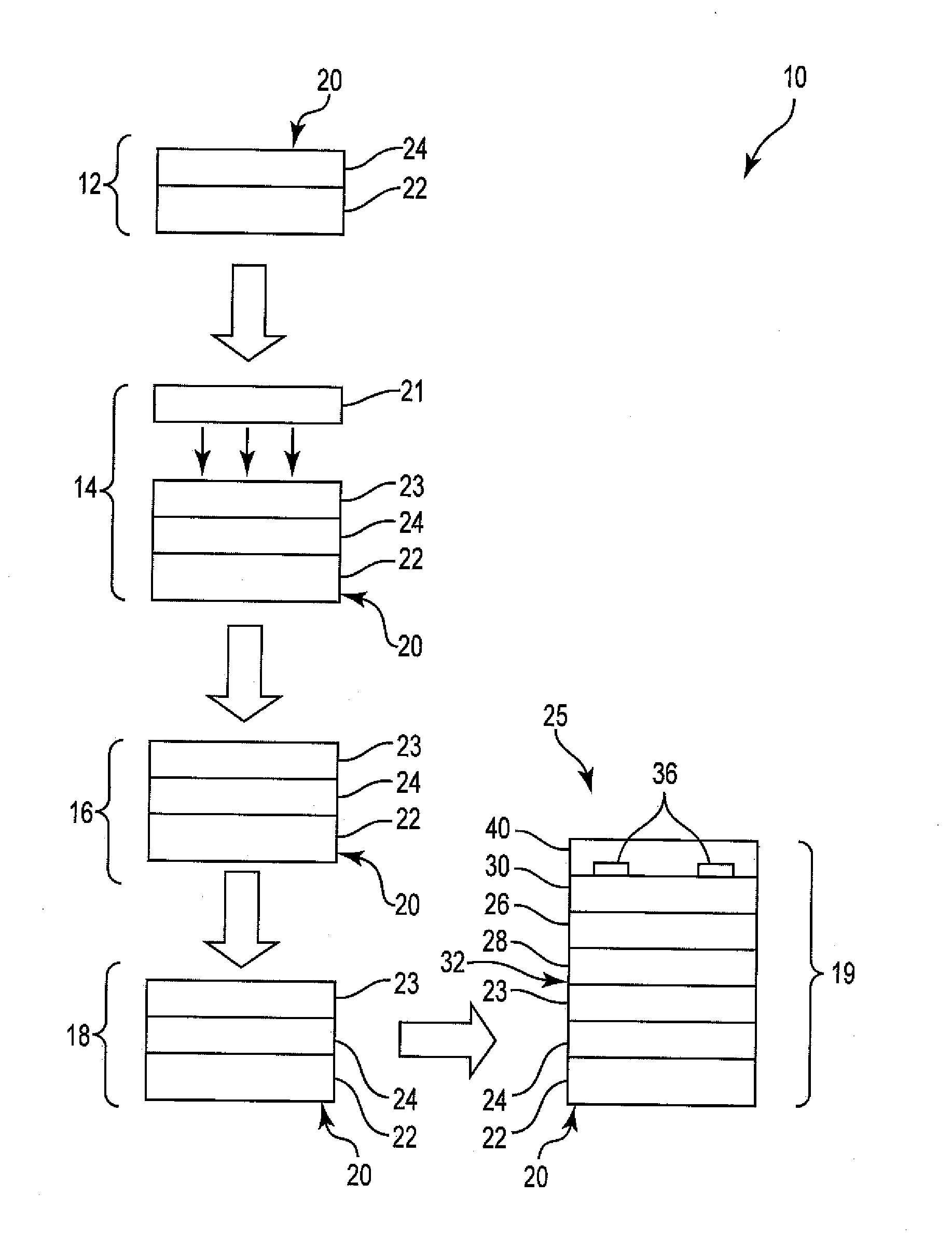
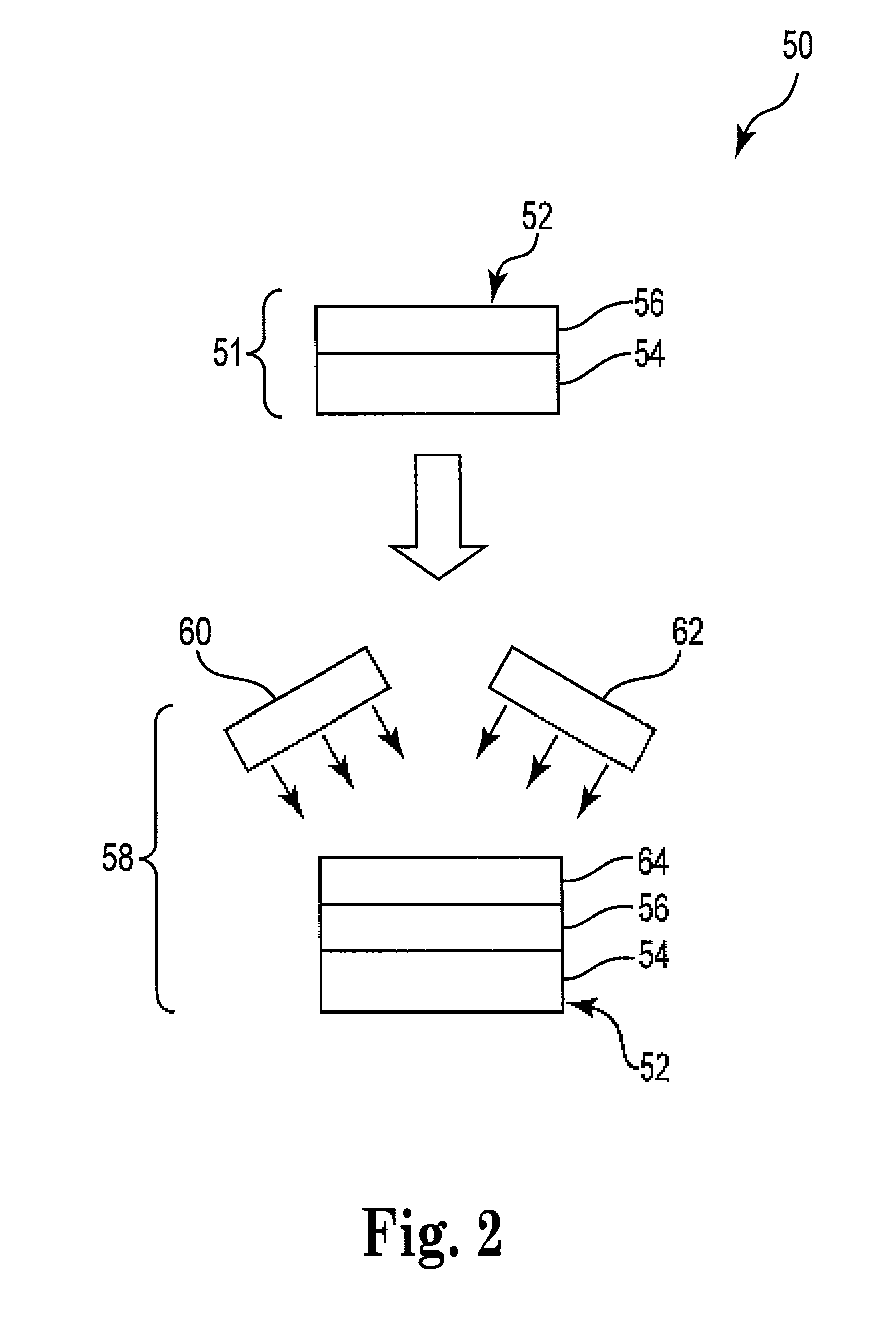
[0106]A precursor film is prepared that has a multilayer format to demonstrate the back-side layer benefit of an Se-containing precursor. The precursor is deposited by first using a CIGS target, (the same CIGS target used for example 2), to deposit a layer for 28% of the total deposition time, with the reminder of the film deposited from a metallic CIG alloy target,(the same CIG target used for example 2). The total time of deposition is 46 minutes, and the power on both targets is 100 W. These depositions are performed at room temperature, using a gas pressure of 5 mTorr. The two sputter sources are arranged in a confocal geometry, and similar pulsed DC sputtering conditions and target-to-substrate conditions are used as Examples 1 and 2. The substrate is also similar to the substrate of example 2, being a 5×5″ piece of stainless steel, coated with Nb (150 nm) and Mo (350 nm) prior to the precursor deposition. The precurso...


PUM

PropertyMeasurementUnit
Fractionaaaaaaaaaa
Fractionaaaaaaaaaa
Thicknessaaaaaaaaaa

Abstract

The present invention provides strategies for making high quality CIGS photoabsorbing materials from precursor films that incorporate a sub-stoichiometric amount of chalcogen(s). Chalcogen(s) are incorporated into the CIGS precursor film via co-sputtering with one or more other constituents of the precursor. Optional annealing also may be practiced to convert precursor into more desirable chalcopyrite crystalline form in event all or a portion of the precursor has another constitution. The resultant precursors generally are sub-stoichiometric with respect to chalcogen and have very poor electronic characteristics. The conversion of these precursors into CMS photoabsorbing material via chalcogenizing treatment occurs with dramatically reduced interfacial void content. The resultant CIGS material displays excellent adhesion to other layers in the resultant photovoltaic devices. Ga migration also is dramatically reduced, and the resultant films have optimized Ga profiles in the top or bottom portion of the film that improve the quality of photovoltaic devices made using the films.

Description

PRIORITY[0001]The present nonprovisional patent application claims priority under 35 U.S.C. §119(e) from United States Provisional patent application having Ser. No. 61 / 314,840, filed on Mar. 17, 2010, by Gerbi et al. and titled CHALCOGENIDE-BASED MATERIALS AND IMPROVED METHODS OF MAKING SUCH MATERIALS, wherein the entirety of said provisional patent application is incorporated herein by reference.FIELD OF THE INVENTION[0002]The present invention relates to methods for making chalcogenide-based photoabsorbing materials as well as to photovoltaic devices that incorporate these materials. More specifically, the present invention relates to methods for making chalcogenide-based photoabsorbing materials, desirably in the form of thin films as well as to photovoltaic devices that incorporate these materials, in which a precursor film incorporating a sub-stoichiometric amount of chalcogen is prepared and then converted to the desired photoabsorbing composition via a chalcogenization treat...

Claims


Application Information

Patent Timeline
IPC IPC(8): H01L31/0264C23C14/34C23C14/06G02F1/361
CPCC23C14/0623C23C14/3464H01L21/02631H01L21/02568H01L21/02614C23C14/5866Y02E10/541Y02P70/50H01L31/0324H01L31/03923H01L31/0749
Inventor GERBI, JENNIFER E.LANGLOIS, MARC G.NILSSON, ROBERT T.
Owner DOW GLOBAL TECH LLC
Why Eureka
Try Eureka