Photovoltaic devices with depleted heterojunctions and shell-passivated nanoparticles

a photovoltaic device and heterojunction technology, applied in the field of photovoltaic cells and quantum dots, to achieve the effects of less susceptible, better defined, and easy passivation

Active Publication Date: 2011-10-06
THE GOVERNINIG COUNCIL OF THE UNIV OF TORANTO
View PDF8 Cites 10 Cited by
  • Summary
  • Abstract
  • Description
  • Claims
  • Application Information

AI Technical Summary

Benefits of technology

[0009]Particular embodiments of photovoltaic devices within the scope of this invention offer further advantages over photovoltaic devices of the prior art. For example, the use of a metal oxide as the electron-accepting layer allows the device to be configured with the electron-accepting layer as the front surface of the device or as the layer that the solar rays first penetrate upon entering the two semiconductor layers that form the photovoltaic junction. The electrons liberated by the rays are thus less susceptible to recombination with the holes since the electrons in these embodiments have a shorter distance to travel before reaching their destination electrode. Also, in embodiments in which the junction is that between a metal oxide and quantum dots, the junction is better defined and easier to passivate, and thus less susceptible to defects, than a metal-semiconductor Schottky junction. This avoids the occurrence of Fermi-level pinning at the interface. Still further, these embodiments present less of a barrier to hole injection than a Schottky device by introducing a large discontinuity in the valence band and by minimizing the electron density at the interface.
[0010]It has further been discovered that the performance of nanocrystals in photovoltaic devices and in optoelectronic devices in general, and particularly nanocrystals with surface anions, is enhanced by depositing cations over the nanocrystals to faun a first or inner shell and deposing anions over the first shell to form a second or outer shell. The inner and outer shells together passivate surface defects on the nanocrystal which tend to disrupt the quantum confinement of the nanocrystal. Passivation is known to be achievable by the placement of short organic ligands such as ethanedithiol, butylamine, or mercaptopropionic acid on the nanocrystal surface. The use of cation and anion shells in place of these ligands offers the advantages that the cation shells bind to the anions on the nanocrystal surface rather than to the cations, as organic ligands tend to do, and the ionic bonds are stable upon exposure to air and light, and particularly moisture, oxygen, and heat. Further advantages of these cation and anion shells are that by avoiding the need for organic ligands, these shells allow the nanocrystals to reside very close to each other in the light-absorbing film and thereby promote electron wave function overlap and carrier mobility, valuable features that are typically impeded by organic ligands.

Problems solved by technology

The inner and outer shells together passivate surface defects on the nanocrystal which tend to disrupt the quantum confinement of the nanocrystal.

Method used


Image

  • Photovoltaic devices with depleted heterojunctions and shell-passivated nanoparticles
  • Photovoltaic devices with depleted heterojunctions and shell-passivated nanoparticles
  • Photovoltaic devices with depleted heterojunctions and shell-passivated nanoparticles

Examples


example 1

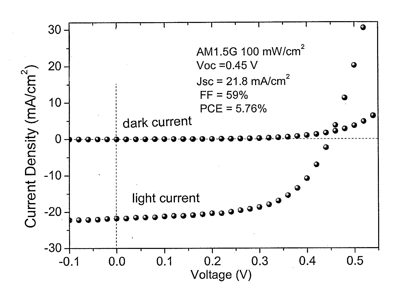
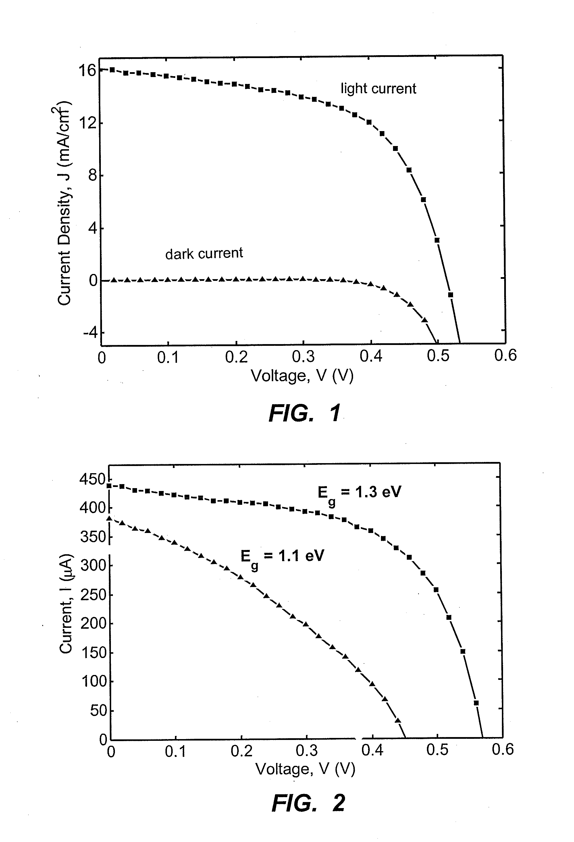
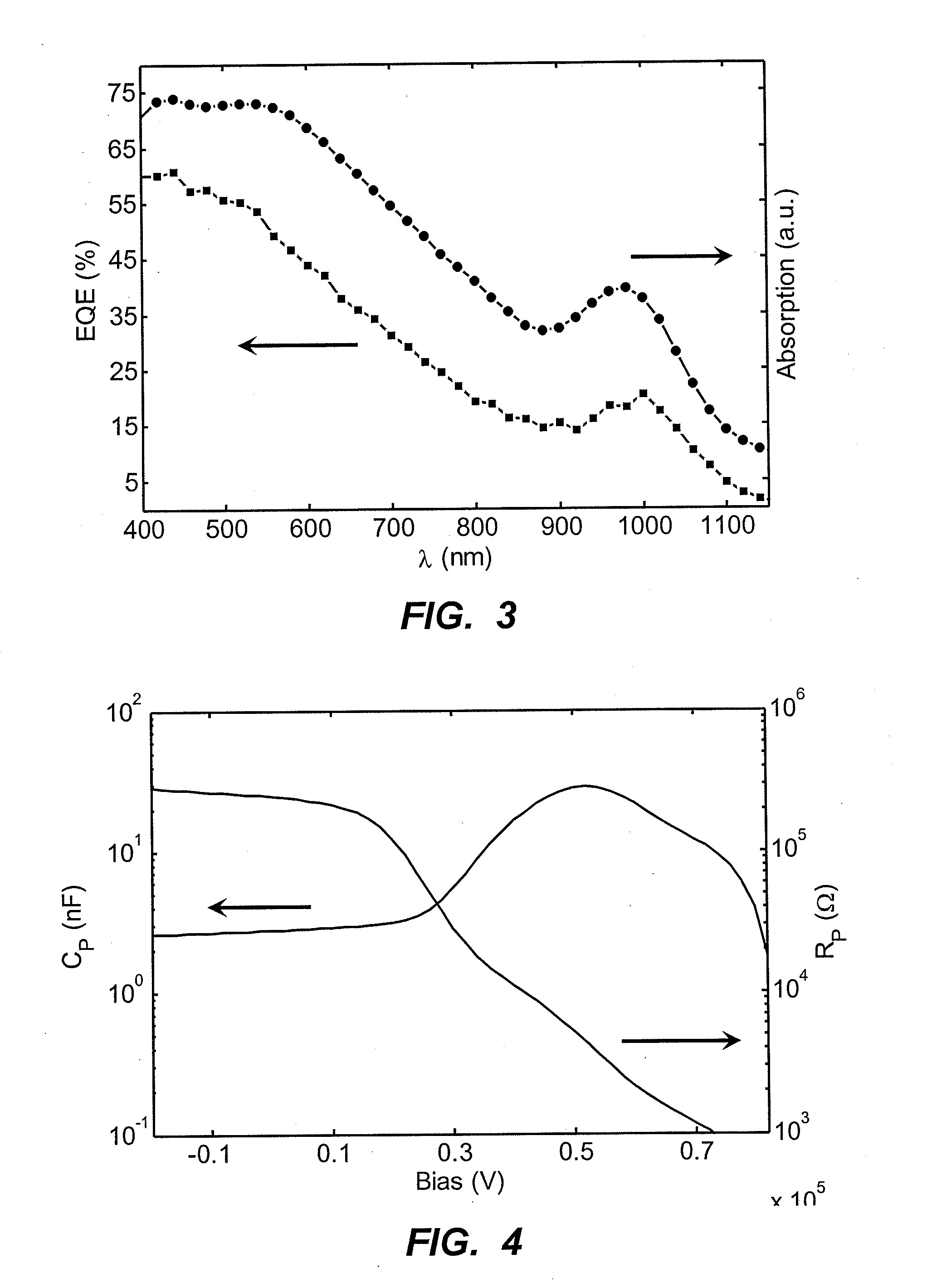
[0025]This example illustrates the preparation of depleted heterojunction photovoltaic cells within the scope of the present invention, each formed by depositing a layer of PbS colloidal quantum dots (approximately 1017 cm−3 n-type doping) of varying diameters—3.7 nm (bandgap 1.3 eV), 4.3 nm (bandgap 1.1 eV), and 5.5 nm (bandgap 0.9 eV)—over transparent TiO2 electrodes.

[0026]The TiO2 electrodes were prepared on SnO2:F (FTO)-coated glass substrates (Pilkington TEC 15, Hartford Glass, Inc., Hartford City, Ind., USA) with a TiO2 paste (DSL-90T, Dyesol Ltd., Queanbeyan, NSW, Australia) as follows. The FTO substrates were first rinsed with toluene, then sonicated for twenty minutes in a mixture of Triton in de-ionized water (1-3% by volume). Separately, a TiO2 paste was prepared by combining one part by weight TiO2 nanoparticles with three parts by weight terpineol. The paste was then spin cast at 1500 rpm for ninety seconds on the TiCl4-treated FTO substrates. One edge of each substrate...

example 2

[0033]This example illustrates the preparation and use of nanoparticles containing a quantum dot core, an inner shell of cations and an outer shell of anions, within the scope of the present invention.

[0034]Colloidal quantum dots capped with oleic acid ligands were synthesized and stripped of their oleate ligands, in the manner described in Example 1. These quantum dots were prepared with an excess of Pb during synthesis, resulting in a lead-rich bulk composition but with sulfur atoms on their surfaces, either from nonpolar {100} and {110} or polar {111} facets in their crystal structure. To form the inner shell of Cd cations over these PbS cores, the nanoparticles were treated with a solution of CdCl2-tetradecylphosphonic acid-oleylamine (CdCl2-TDPA-OLA). This treatment resulted in a slight redshift (between 6 and 24 nm) of the excitonic absorption, suggesting growth of a partial monolayer of highly cation-rich material on the surface, an interpretation reinforced by the approximat...


PUM


Abstract

Photovoltaic cells are fabricated in which the compositions of the light-absorbing layer and the electron-accepting layer are selected such that at least one side of the junction between these two layers is substantially depleted of charge carriers, i.e., both free electrons and free holes, in the absence of solar illumination. In further aspects of the invention, the light-absorbing layer is comprised of dual-shell passivated quantum dots, each having a quantum dot core with surface anions, an inner shell containing cations to passivate the core surface anions, and an outer shell to passivate the inner shell anions and anions on the core surface.

Description

CROSS-REFERENCES TO RELATED APPLICATIONS[0001]This patent application claims the benefit of U.S. Provisional Patent Application No. 61 / 321,450, filed Apr. 6, 2010, and U.S. Provisional Patent Application No. 61 / 334,650, filed May 14, 2010. The contents of both provisional applications are hereby incorporated herein by reference.BACKGROUND OF THE INVENTION[0002]1. Field of the Invention[0003]This invention resides in the fields of photovoltaic cells and quantum dots.[0004]2. Description of the Prior Art[0005]Solar cells that generate electricity through the photovoltaic effect require a combination of low cost and high efficiency in order for such cells to offer a practical alternative to traditional means of power generation. One way in which the cost of manufacturing a photovoltaic cell can be lowered is by the use of solution processing to form the layer of light-harvesting material that is part of the cell. The efficiency of the cell, however, depends on the cell materials, inclu...

Claims


Application Information

Patent Timeline
Patent Type & Authority Applications(United States)
IPC IPC(8): H01L31/072H01L31/0256H01L29/06B82Y99/00
CPCC09K11/661C09K11/662Y02E10/50H01L31/0352H01L31/072H01L31/0324C09K11/02Y10S977/774Y10S977/892Y10S977/948H01L31/02167H01L31/022433H01L31/0236H01L31/02366H01L31/0296H01L31/032H01L31/035218B82Y20/00B82Y40/00H01L31/022466H01L31/1868
Inventor TANG, JIANGPATTANTYUS-ABRAHAM, ANDRASKRAMER, ILLANBARKHOUSE, AARONWANG, XIHUAKONSTANTATOS, GERASIMOSDEBNATH, RATANSARGENT, EDWARD H.
Owner THE GOVERNINIG COUNCIL OF THE UNIV OF TORANTO
Why Eureka
Try Eureka