Photovoltaic Cells With Improved Electrical Contact

a photovoltaic cell and electrical contact technology, applied in the direction of basic electric elements, electrical apparatus, semiconductor devices, etc., can solve the problems of inefficiency, process interruption, and inutility of metal/p-cdte contacts in cell fabrication, and achieve low-resistance contact, improved contact properties, and high efficiency

Inactive Publication Date: 2011-10-06
UNIVERSITY OF ROCHESTER
View PDF10 Cites 34 Cited by
  • Summary
  • Abstract
  • Description
  • Claims
  • Application Information

AI Technical Summary

Benefits of technology

[0007]The present invention provides a device structure for photovoltaic cells. The photovoltaic cells of the present invention have the advantages such as, for example, high efficiency, improved contact properties such as achieving low-resistance contact to the p-type semiconductor layer in photovoltaic cells (e.g., p-CdTe), eliminating a solution processing step in the cell fabrication process and improving the cell fabrication throughput by using a continuous dry process (e.g., in-line physical vapor deposition process) for all the cell layers.

Problems solved by technology

Although it is expected that a high work function metal such as Au or Ni would be useful providing the low-resistance contact to the p-CdTe, in practice such metal / p-CdTe contacts are not useful because they can cause degradation in the solar cell during operation or at elevated temperature due to chemical reaction or metal diffusion.
The solution etching step, which involves dipping the substrate / TCO / CdS / CdTe structure in a nitric / phosphoric acid bath (known as NP treatment) for a short time, necessitates its removal from the vacuum chamber and therefore can, cause process interruption and inefficiency in the cell fabrication.

Method used


Image

  • Photovoltaic Cells With Improved Electrical Contact
  • Photovoltaic Cells With Improved Electrical Contact
  • Photovoltaic Cells With Improved Electrical Contact

Examples


example 1

Comparison of Photovoltaic Cells Fabricated with and without a Back Buffer Layer

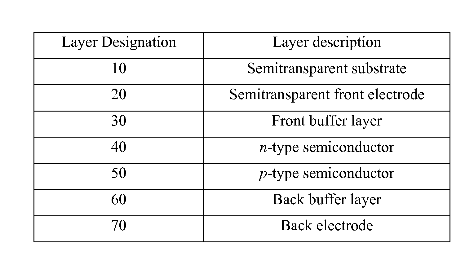
[0054]CdS / CdTe photovoltaic cells were prepared using a process described as follows. Commercially available soda lime glass with SnO2:F coating was used as the substrate. A layer of CdS film was deposited on top of the substrate using chemical bath deposition method as described by Chu et al. in “Solution-Grown Cadmium Sulfide Films for Photovoltaic Devices”, Journal of Electrochemical Society, vol. 139, pp. 2443-2446 (1992). CdTe film was deposited on top of CdS using a close-space sublimation method as described by Tyan in “Topics on Thin Film CdS / CdTe Solar Cells”, Solar Cells, vol. 23, pp. 19-29 (1988). Following the CdTe deposition, a cadmium chloride vapor treatment step was performed in a method as described by McCandless et al. in “Optimization of Vapor Post-deposition Processing for Evaporated CdS / CdTe Solar Cells”, Progress in Photovoltaics, vol. 7, pp. 21-30 (1999). After the cadmium chloride...

example 2

Example of Photovoltaic Cells Fabricated with and without a Nickel Oxide, NiOx, Back Buffer Layer

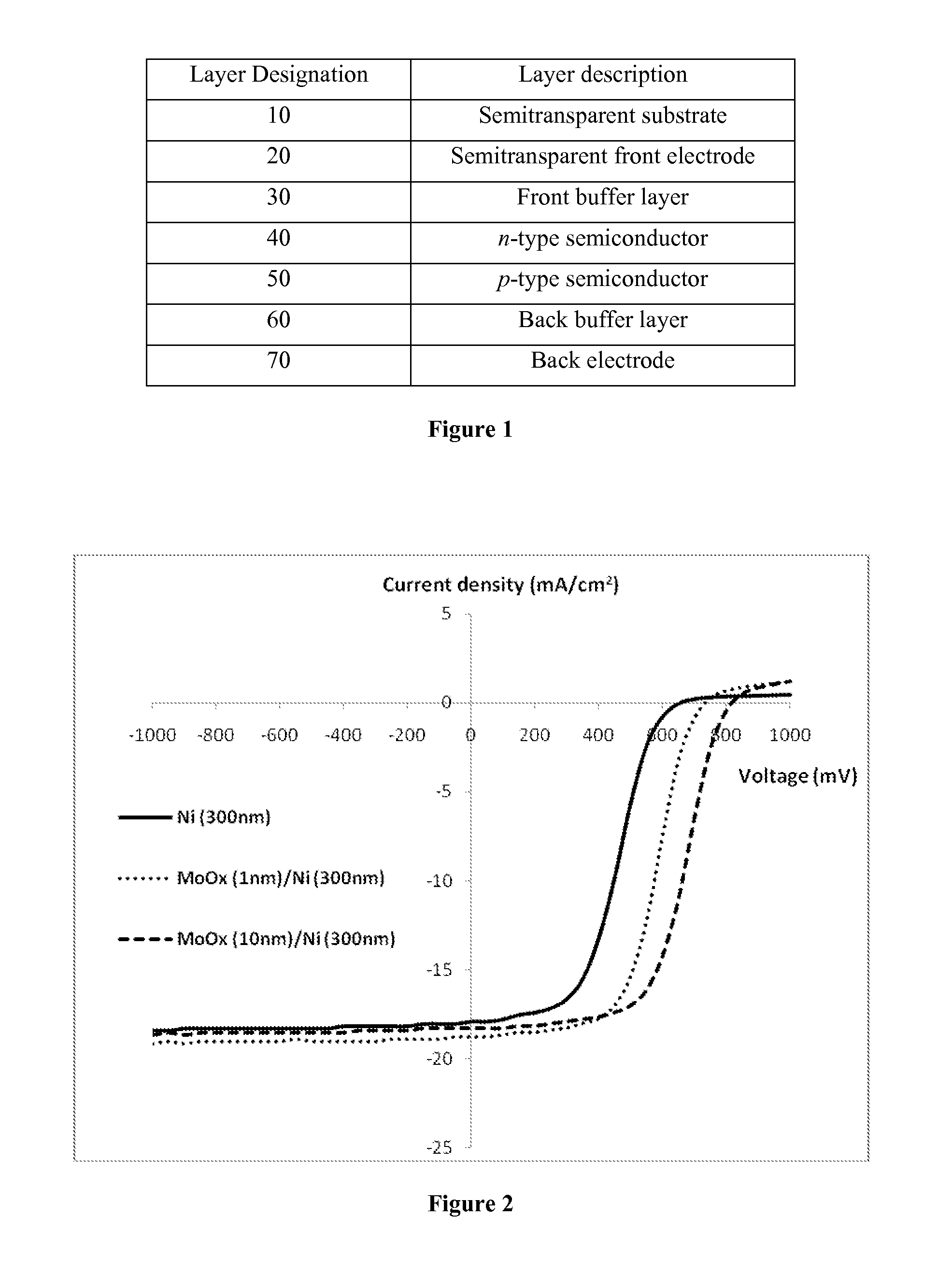
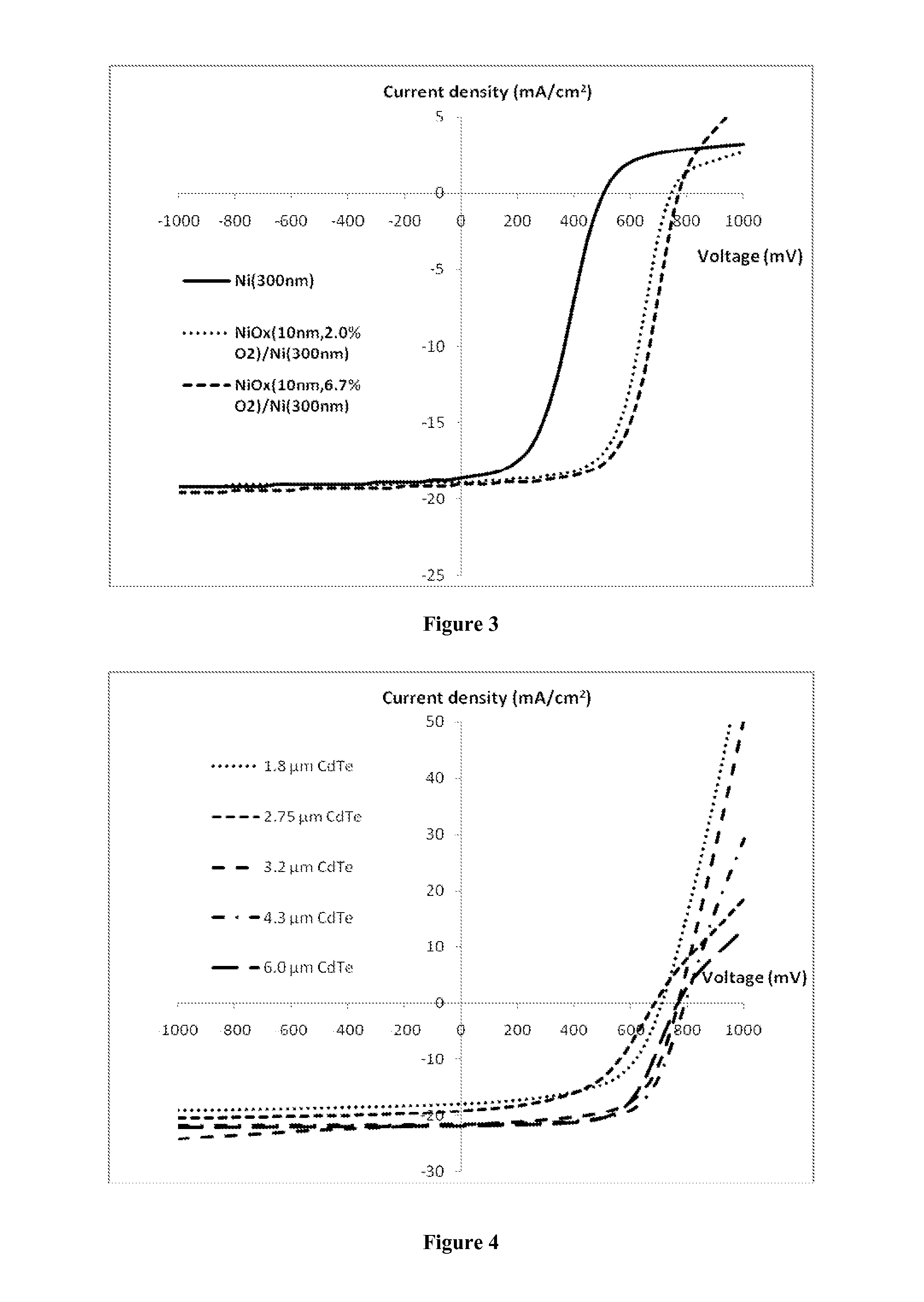
[0057]CdS / CdTe photovoltaic cells were prepared as described in Example 1, except that NiOx was used as the back buffer layer instead of MoOx. The NiOx layer was deposited on top of the p-CdTe layer by reactive sputtering in a mixture of oxygen and argon. FIG. 3 shows the J-V characteristics of a CdS / CdTe reference cell without the NiOx, back buffer layer, a CdS / CdTe cell with 10 nm NiOx deposited in an atmosphere containing 2.0% O2 as the back buffer layer, and a CdS / CdTe cell with 10 nm NiOx deposited in an atmosphere containing 6.7% O2 as the back buffer layer. The performance parameters for these cells are shown in Table 2. It is clear that there are substantial improvements in all performance parameters for cells with a buffer layer of NiOx. The improvement in efficiency over the reference cell is 97% and 109% for cells with two different NiOx buffer layers, respectively.

TABLE 2Devi...

example 3

Control

Back Buffer Layer Produced by NP Treatment

[0058]In this example, the back buffer layer for the CdS / CdTe cell was prepared using the conventional NP treatment. With this treatment, the CdS / CdTe cell was dipped in a mixture of nitric and phosphoric acids for a duration of several tens of seconds to produce a tellurium rich surface on top of the CdTe as the back buffer layer. The back electrode was then applied by vapor deposition to this buffer layer to complete the cell fabrication. FIG. 4 shows the current-voltage characteristics of a series of cells with various CdTe thicknesses from 1.8 to 6.0 μm and a back buffer layer produced by NP treatment.

[0059]Table 3 summarizes the cell performance parameters. It is noted that the VOC, JSC, FF and the overall efficiency are lower for the cells with a thin CdTe layer (2.75 μm and below). Attempts to make cells with a CdTe layer of thickness below 1.8 μm resulted in shorted cells, apparently due to pin-hole formation caused by the sol...


PUM

PropertyMeasurementUnit
work functionaaaaaaaaaa
temperatureaaaaaaaaaa
thicknessaaaaaaaaaa

Abstract

A photovoltaic cell comprising a metal oxide back buffer layer. Improved n-CdS / p-CdTe heterojunction photovoltaic cells comprising a metal oxide buffer layer for making low-resistance electrical contact to the p-type CdTe layer. The back buffer layer comprises metal oxides having a high work function.

Description

FIELD OF THE INVENTION[0001]The present invention generally relates to the structure and production of photovoltaic cells. More particularly, the invention relates to structure of and production of CdS / CdTe thin-film photovoltaic cells.BACKGROUND OF THE INVENTION[0002]Polycrystalline n-CdS / p-CdTe heterojunction solar cells are attractive for large-scale, terrestrial electricity generation. In order to achieve high efficiency in a solar cell, the CdS / CdTe heterojunction structure is often subjected to additional bulk and surface treatments subsequent to the deposition of the CdS and CdTe layers. These treatment steps are needed to improve the crystalline quality of the CdTe thin film and to produce a chemically modified CdTe surface for making ohmic or low-resistance electrical contact.[0003]An established process suitable for the manufacture of high-efficiency CdS / CdTe solar cells is as follows: in sequence, CdS and CdTe layers are deposited in a vacuum chamber by a close-space subl...

Claims


Application Information

Patent Timeline
Patent Type & Authority Applications(United States)
IPC IPC(8): H01L31/00
CPCH01L31/0296H01L31/0392Y02E10/543H01L31/1836H01L31/073H01L31/03925
Inventor LIN, HAOXIA, WEIWU, HSIANG NINGTANG, CHING WAN
Owner UNIVERSITY OF ROCHESTER
Why Eureka
Try Eureka