Field effect transistor, method for manufacturing the same, and sputtering target

a field effect transistor and sputtering target technology, applied in the direction of electrolysis components, vacuum evaporation coatings, coatings, etc., can solve the problems of difficult application of the field effect transistor to a large-area substrate, large amount of energy and a large number of steps, and large amount of production steps. , to achieve the effect of reducing the number of masks, and reducing the production cos

Active Publication Date: 2011-10-06
IDEMITSU KOSAN CO LTD
View PDF8 Cites 82 Cited by
  • Summary
  • Abstract
  • Description
  • Claims
  • Application Information

AI Technical Summary

Benefits of technology

[0108]There are no particular restrictions on the material for forming the protective layer. Materials which are commonly used can be selected arbitrarily within a range which does not impair advantageous effects of the invention. For example, compounds such as SiO2, SiNx, Al2O3, Ta2O5, TiO2, MgO, ZrO2, CeO2, K2O, Li2O, Na2O, Rb2O, Sc2O3, Y2O3, Hf2O3, CaHfO3, PbTi3, BaTa2O6, SrTiO3, AlN or the like may be used. Of these, it is preferable to use SiO2, SiNx, Al2O3, Y2O3, Hf2O3 and CaHfO3, with SiO2, SiNx, Y2O3, Hf2O3 and CaHfO3 being more preferable. It is particularly preferred that the protective layer be formed of an oxide, and oxides such as SiO2, Y2O3, Hf2O3 and CaHfO3 are preferable. The oxygen number of these oxides may not necessarily coincide with the stoichiometrical ratio (for example, they may be SiO2 or SiOx). SiNx may contain a hydrogen element.
[0109]Such a protective layer may be a stack structure in which two or more different insulating films are stacked.
[0110]The protective layer may be crystalline, polycrystalline or amorphous. It is preferred that the layer be polycrystalline or amorphous since it can be produced easily on the industrial scale. In particular, it is preferred that the protective layer be amorphous. If the protective layer is an amorphous film, the interface has good smoothness, and as a result, improvement in mobility, suppression of the threshold voltage and suppressive effects of the S value can be expected. Further, gate current leakage can be suppressed.
[0111]It is preferred that the protective layer of the semiconductor layer be an amorphous oxide or an amorphous nitride, with an amorphous oxide being particularly preferable. If the protective layer is not an oxide, oxygen in the semiconductor moves toward the protective layer, and as a result, the off current may be increased or the threshold voltage may be negative to cause the transistor to be normally-off. An organic insulating film such as poly(4-vinylphenol)(PVP) or parylene may be used in the protective layer of the semiconductor layer. Further, the protective layer of the semiconductor layer may have a stack structure in which an inorganic insulating film and an organic insulating film are stacked in two or more.
[0112]In particular, it is preferred that the first protective layer which is largely in contact with the semiconductor layer and that the second protective layer be formed of a nitride such as SiNx. Due to such a configuration, good transistor characteristics and moisture resistance can be easily attained.
[0113]Although the protective layer can be formed by PECVD, TEOSCVD, Cat-CVD, sputtering, spin-coating, the printing method, or the like, PECVD or sputtering is industrially preferable, with PECVD being particularly preferable.4. Gate Insulating Film

Problems solved by technology

Therefore, it is difficult to apply it to a large-area substrate.
In addition, there is a problem that a large amount of energy and a large number of steps are required in production.
Further, since crystalline silicon is normally restricted to a TFT with a top-gate configuration, a reduction in production cost such as a decrease in number of masks is difficult.
Therefore, a problem may arise that a large-area, highly precise and high-frequency animation cannot be displayed.
Further, there is a problem that a field effect transistor using amorphous silicon has low stability (reliability) to direct current stress and hence it is difficult to apply it to a self-emission type display element such as an organic EL device which is driven at direct current.
However, of such metal oxide semiconductors, a conventional metal oxide semiconductor using zinc oxide has poor TFT characteristics such as a low mobility, a small on-off ratio, a large amount of current leakage, unclear pinch-off and tendency of becoming normally-on.
In addition, due to poor chemicals resistance, metal oxide semiconductors have problems that they are hard to be subjected to wet etching or the like, and hence, the production process or the use environment was restricted.
Furthermore, since it is required to form an oxide semiconductor into a film at a high pressure in order to improve performance, the film-forming speed is slow and a high temperature treatment at 700° C. or higher is required.
Moreover, in the case of a semiconductor with a top-gate configuration, many restrictions are imposed for practical use since the film thickness of the oxide semiconductor is required to be 50 nm or more.
However, if gallium (Ga) is not added, stability to environments such as moisture resistance is lowered, and when the added amount of Ga increased, there is a possibility that the TFT characteristics, such as mobility and S value, may be deteriorated.
Moreover, since Ga is a costly rare metal, stable supply thereof is difficult.
Although a field effect transistor using tin oxide has been studied for many years, it has not been put in practical use due to a high off current and a low mobility.
For these reasons, it is considered that tin oxide is not suitable as a semiconductor material.
Furthermore, although the mobility can be improved by a heat treatment, since the threshold voltage tends to shift in the negative direction greatly according to a heat treatment temperature, there were problems which inhibit practical use such as a large variation in properties of each transistor, poor reliability or the like (for example, see Non-Patent Document 1).
For these reasons, it is believed that it is difficult to find out a composition ratio which can produce a field effect transistor with excellent transistor characteristics (for example, see Non-Patent Document 2).

Method used


Image

  • Field effect transistor, method for manufacturing the same, and sputtering target
  • Field effect transistor, method for manufacturing the same, and sputtering target
  • Field effect transistor, method for manufacturing the same, and sputtering target

Examples


examples 1 to 17

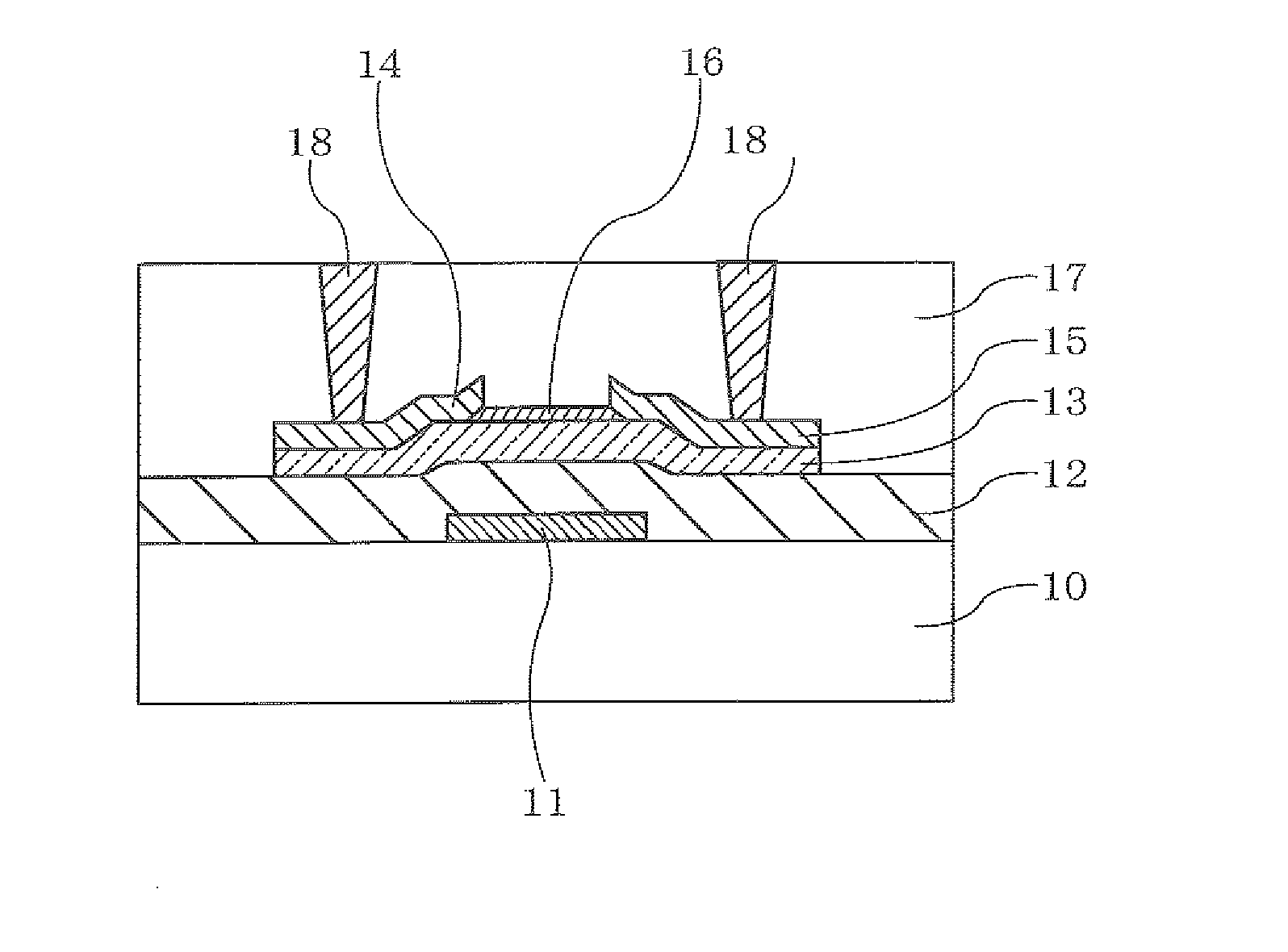
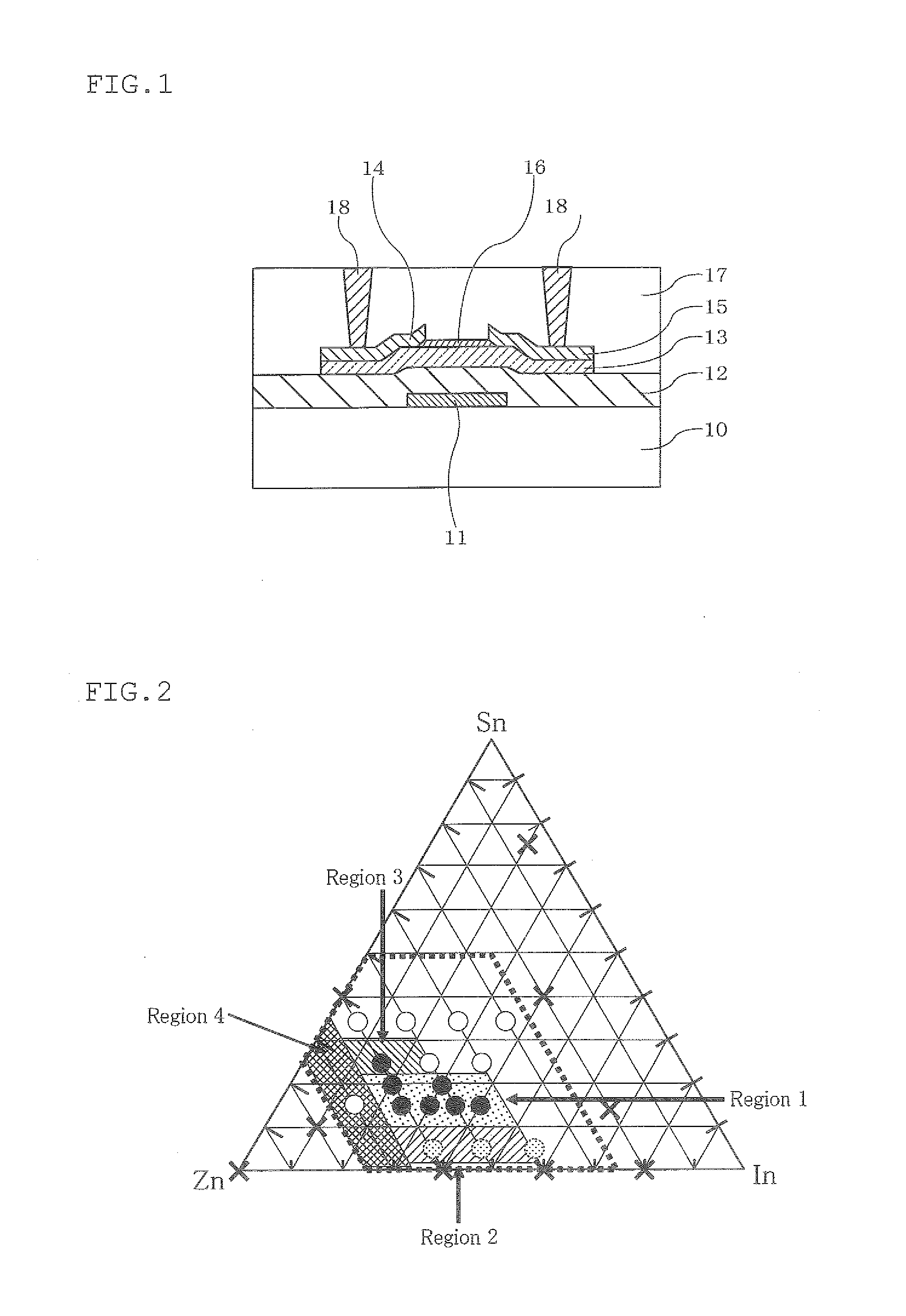
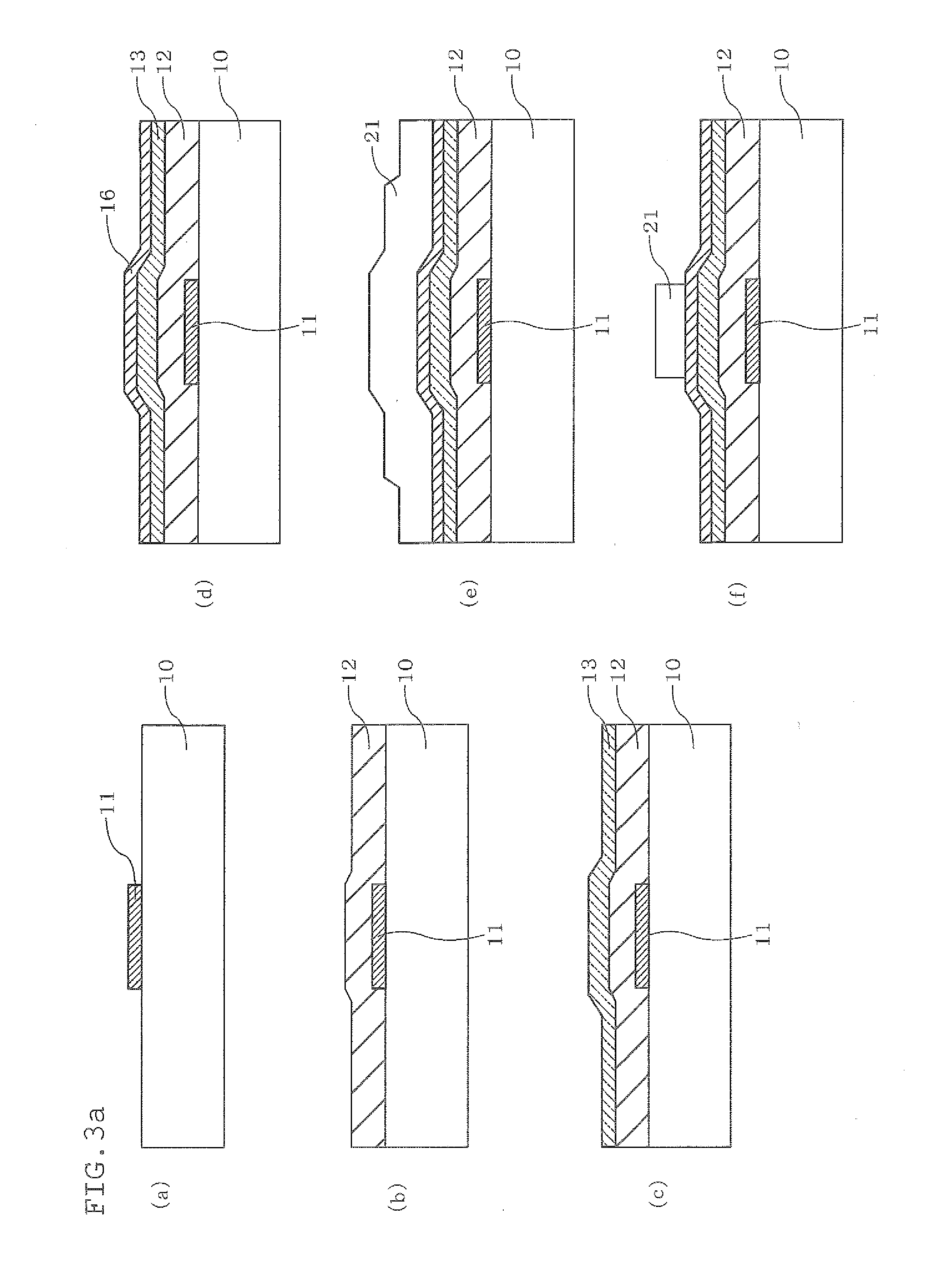
[0212]An etch-stopper (ES) type field effect transistor with a bottom-gate structure shown in FIG. 1 was fabricated. The production process will be explained below with reference to the drawings.

[0213]FIGS. 3a and 3b each show the steps of producing the field effect transistor.

[0214]On a glass substrate 10, metal molybdenum was formed in a thickness of 200 nm by RF sputtering at room temperature, followed by patterning by wet etching to prepare a gate electrode 11 (FIG. 3a(a)).

[0215]Next, by a plasma-enhanced chemical vapor deposition (PECVD) apparatus, SiOx was formed into a film on the substrate on which the gate electrode 11 was provided, thereby to form a gate insulating film 12 (FIG. 3a(b)).

[0216]Next, the targets for a semiconductor layer produced in Evaluation Examples 1 to 17 were mounted in a film-forming apparatus of the DC magnetron sputtering method, which is one of the DC sputtering methods, and a semiconductor layer 13 (film thickness: 30 nm) was formed on the gate ins...

examples 18 to 25

[0230]Transistors were fabricated and evaluated in the same manner as in Example 1, except that the semiconductor layer was formed at the same conditions as those in Evaluation Examples shown in Tables 4 and 5. The results are shown in Table 7.

examples 26 to 32

[0231]Transistors were fabricated and evaluated in the same manner as in Example 1, except that the formation of the semiconductor layer and the source / drain electrodes were changed as shown in Tables 4 and 5, and the formation of the semiconductor layer and the formation of the source / drain electrodes were conducted by wet etching.

[0232]The semiconductor layer was patterned by using an oxalic acid-based etching solution, and the source electrode and the drain electrode were patterned by using a PAN-based etching solution.


PUM

PropertyMeasurementUnit
threshold voltageaaaaaaaaaa
off currentaaaaaaaaaa

Abstract

A field effect transistor including: a substrate, and at least gate electrode, a gate insulating film, a semiconductor layer, a protective layer for the semiconductor layer, a source electrode and a drain electrode provided on the substrate, wherein the source electrode and the drain electrode are connected with the semiconductor layer therebetween, the gate insulating film is between the gate electrode and the semiconductor layer, the protective layer is on at least one surface of the semiconductor layer, the semiconductor layer includes an oxide containing In atoms, Sn atoms and Zn atoms, the atomic composition ratio of Zn / (In+Sn+Zn) is 25 atom % or more and 75 atom % or less, and the atomic composition ratio of Sn / (In+Sn+Zn) is less than 50 atom %.

Description

TECHNICAL FIELD[0001]The invention relates to a field effect transistor, a method for manufacturing the same and a sputtering target.BACKGROUND ART[0002]A field effect transistor is a device which is widely used as a unit electronic element of a semiconductor memory integrated circuit, a high-frequency signal amplification element, a liquid crystal driving element or the like. It is an electronic device which is most practically used in recent years.[0003]Of these, in particular, with a remarkable progress in displays in recent years, a thin film transistor (TFT) is widely used as a switching device which applies a voltage to a display element to drive a display for liquid crystal displays (LCD), electroluminescence displays (EL) and field emission displays (FED).[0004]As the material of the above-mentioned thin film transistor, a silicon-based semiconductor is widely used. In general, crystalline silicon is used in a high-frequency amplification element, an integrated circuit eleme...

Claims


Application Information

Patent Timeline
Patent Type & Authority Applications(United States)
IPC IPC(8): H01L29/786H01L21/36H01L29/22C23C14/08
CPCH01L29/78609H01L29/66969H01L29/7869H01L29/78633H01L29/78606C23F1/20C22C30/04C22C30/06H01L29/78696H01L29/06H01L29/66742C23C14/3407C23C14/165H01L27/1225H01L21/02565H01L21/02554H01L29/78693
Inventor YANO, KOKIKAWASHIMA, HIROKAZUINOUE, KAZUYOSHI
Owner IDEMITSU KOSAN CO LTD
Why Eureka
Try Eureka