Apparatus with a Multi-Layer Coating and Method of Forming the Same

a multi-layer coating and apparatus technology, applied in the field of polymer coatings, can solve the problems of reducing the lifetime of such joints, reducing the service life of such joints, so as to prevent preventing or hindering the soldering of an electrical component, and preventing the oxidation of the conductive tracks on the pcb

Active Publication Date: 2011-10-20
HZO INC
View PDF3 Cites 43 Cited by
  • Summary
  • Abstract
  • Description
  • Claims
  • Application Information

AI Technical Summary

Benefits of technology

[0037]Applying the coating to a PCB or other device may provide several advantages. Various embodiments may have none, some, or all of these advantages. One advantage is that the coating may prevent conductive tracks on a PCB from oxidizing. A PCB is often stored for some period of time before electrical components are soldered to the PCB. If the PCB is uncoated, the conductive tracks on the PCB may oxidize during storage. An oxidation layer on a conductive track may prevent or hinder the soldering of an electrical component to the conductive track. By applying the coating to the PCB prior to storage, a manufacturer may prevent the conductive tracks on the PCB from oxidizing. By preventing oxidation, the coating may permit the formation of strong solder joints on the PCB.
[0038]Another advantage is that the coating may allow an electrical component to be soldered through the coating without the prior removal of the coating. The coating may comprise one or more halo-hydrocarbon polymers. In some embodiments, the heat, solder, and/or flux applied during the soldering process may selectively alter the coating on the particular area of the PCB where the solder joint is to be formed. In some embodiments, the soldering process may remove the coating only in the area of the solder joint. Accordingl

Problems solved by technology

The metal surfaces on the electrical components and PCBs often oxidize or corrode before being soldered together.
The oxidation or corrosion of the metal surfaces may prevent

Method used


Image

  • Apparatus with a Multi-Layer Coating and Method of Forming the Same
  • Apparatus with a Multi-Layer Coating and Method of Forming the Same
  • Apparatus with a Multi-Layer Coating and Method of Forming the Same

Examples


Embodiment Construction

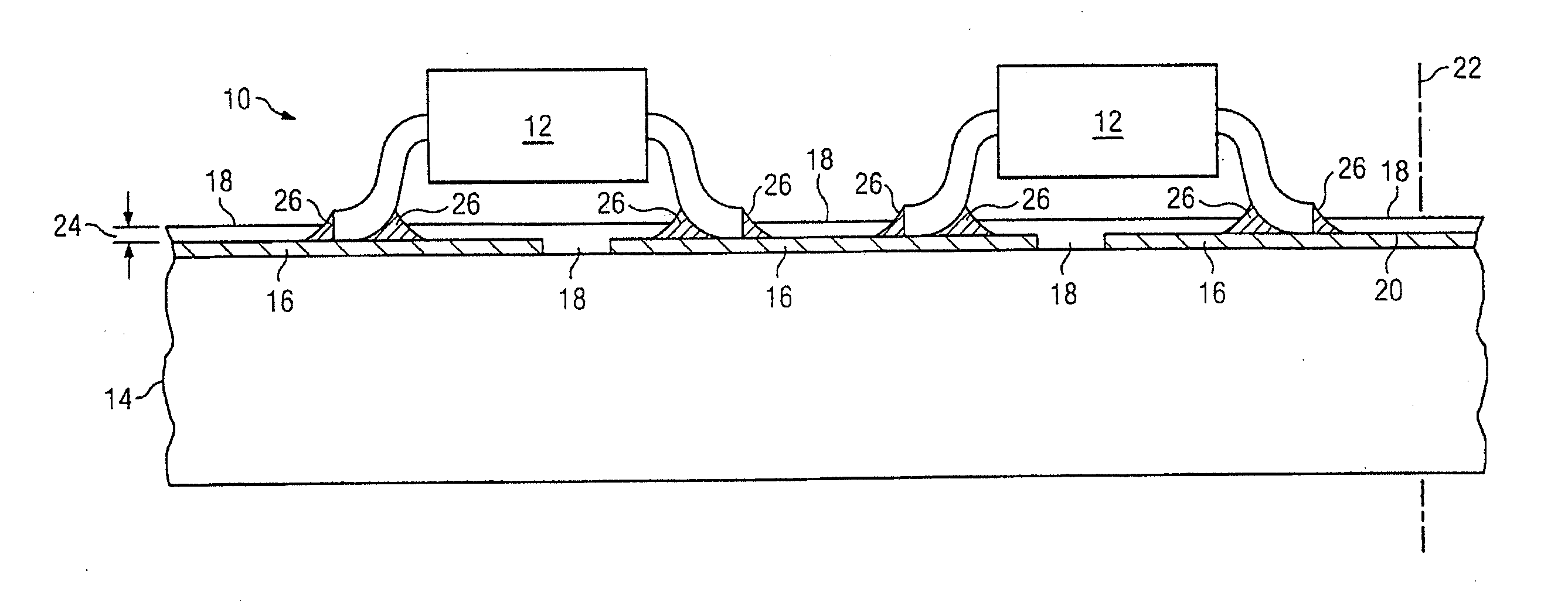
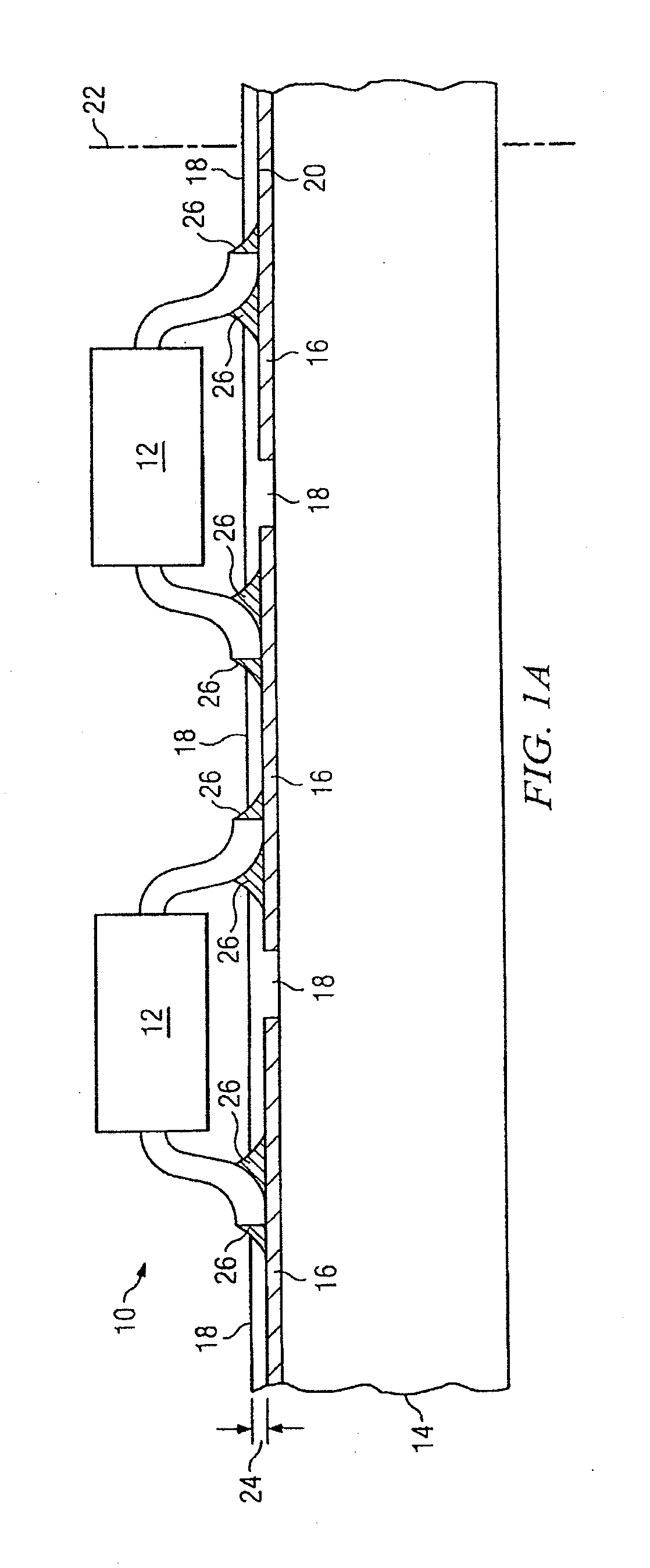
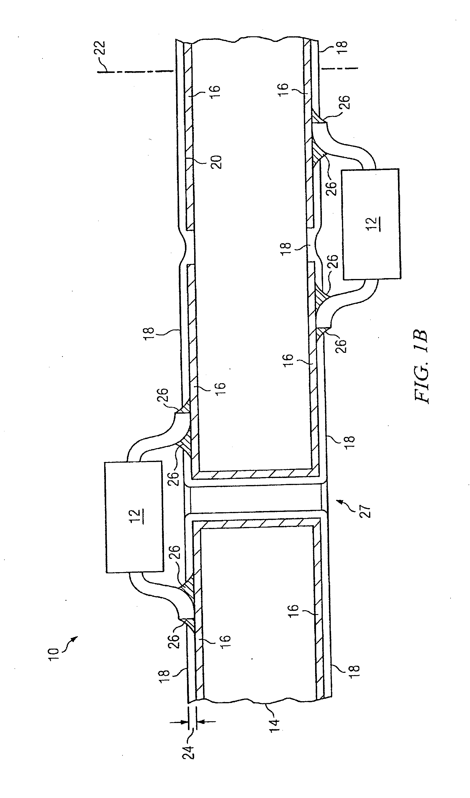
[0057]FIG. 1A illustrates a printed circuit board (PCB) 10, according to certain embodiments. PCB 10 may mechanically support and / or electrically connect one or more electrical components 12 associated with an electrical circuit. PCB 10 may comprise a substrate 14, one or more conductive tracks 16, a coating 18, and one or more electrical components 12.

[0058]Substrate 14 in PCB 10 may comprise one or more boards that mechanically support elements of a circuit. For example, conductive tracks 16 and / or electrical components 12 may be affixed to at least one surface of substrate 14. Substrate 14 may comprise any suitable insulating material that prevents substrate 14 from shorting the circuit of PCB 10. In some embodiments, substrate 14 in PCB 10 comprises an epoxy laminate material, a synthetic resin bonded paper, an epoxy resin bonded glass fabric (ERBGH), a composite epoxy material (CEM), a phenolic cotton paper, and / or any other suitable type and / or combination of insulating materi...


PUM

PropertyMeasurementUnit
Thicknessaaaaaaaaaa
Thicknessaaaaaaaaaa
Thicknessaaaaaaaaaa

Abstract

In some embodiments, a printed circuit board (PCB) comprises a substrate comprising an insulating material. The PCB further comprises a plurality of conductive tracks attached to at least one surface of the substrate. The PCB further comprises a multi-layer coating deposited on the at least one surface of the substrate. The multi-layer coating (i) covers at least a portion of the plurality of conductive tracks and (ii) comprises at least one layer formed of a halo-hydrocarbon polymer. The PCB further comprises at least one electrical component connected by a solder joint to at least one conductive track, wherein the solder joint is soldered through the multi-layer coating such that the solder joint abuts the multi-layer coating.

Description

RELATED APPLICATIONS[0001]The present application is a U.S. National Stage Application of International Application No. PCT / GB2009 / 001966, filed Aug. 11, 2009 entitled “Halo-Hydrocarbon Polymer Coating,” which claims priority to United Kingdom Application No. GB 0815094.8, filed Aug. 18, 2008, entitled “Wire Bonding;” United Kingdom Application No. GB 0815095.5, filed Aug. 18, 2008, entitled “Devices;” and United Kingdom Application No. GB 0815096.3 filed Aug. 18, 2008, entitled “Printed Circuit Boards.”TECHNICAL FIELD OF THE INVENTION[0002]This disclosure relates generally to polymer coatings and, more specifically, to a halo-hydrocarbon polymer coating for electrical devices.BACKGROUND OF THE INVENTION[0003]Many electrical devices comprise electrical components that are soldered to printed circuit boards (PCBs). The metal surfaces on the electrical components and PCBs often oxidize or corrode before being soldered together. The oxidation or corrosion of the metal surfaces may prev...

Claims


Application Information

Patent Timeline
IPC IPC(8): H05K1/03B23K31/02H05K3/00H05K1/00
CPCH01L2924/01049H01L2924/0105H01L2924/01051H01L2924/01074H01L2924/01077H01L2924/01078H01L2924/01079H01L2924/01082H01L2924/01083H01L2924/01327H01L2924/014H01L2924/14H01L2924/19042H01L2924/19043H01L2924/2075H01L2924/20751H01L2924/20752H01L2924/20753H01L2924/20754H01L2924/20755H01L2924/20756H01L2924/20757H01L2924/3011H05K3/222H05K3/282H05K3/284H05K3/328H05K2201/015H05K2201/0179H05K2201/0195H05K2203/049H01L2924/01019H01L2924/01021H01L2924/01023H01L2924/01024H01L2924/01045H01L2924/01072H01L2924/01087H01L24/85H01L2224/8502Y10T29/49155H01L2924/19107H01H13/78H01H2215/004H01H2229/012H01L24/45H01L24/48H01L2224/45014H01L2224/45015H01L2224/45105H01L2224/45109H01L2224/45111H01L2224/45113H01L2224/45116H01L2224/4512H01L2224/45124H01L2224/45139H01L2224/45144H01L2224/45147H01L2224/45149H01L2224/45155H01L2224/45157H01L2224/4516H01L2224/45164H01L2224/45166H01L2224/45169H01L2224/4517H01L2224/45171H01L2224/45173H01L2224/45178H01L2224/4518H01L2224/45184H01L2224/45565H01L2224/45599H01L2224/45644H01L2224/48091H01L2224/48455H01L2224/48463H01L2224/48464H01L2224/48599H01L2224/48699H01L2224/85201H01L2224/85205H01L2924/01005H01L2924/01006H01L2924/01007H01L2924/01011H01L2924/01013H01L2924/01014H01L2924/01015H01L2924/01016H01L2924/01018H01L2924/01022H01L2924/01025H01L2924/01027H01L2924/01028H01L2924/01029H01L2924/0103H01L2924/01031H01L2924/01032H01L2924/01033H01L2924/0104H01L2924/01042H01L2924/01046H01L2924/01047H01L2924/00014H01L2924/00H05K2203/1322H01L2924/12042H01L2224/45138H01L2224/06H01L2224/4569H01L2224/85439H01L2224/85444H01L2224/85447H01L2224/85484H01L2224/85611H01L2924/20759H01L2924/2076H01L2924/20758H01L2924/206H01L2224/43848H05K3/28H05K1/0353
Inventor HUMPHRIES, MARK ROBSONFERDINANDI, FRANKSMITH, RODNEY EDWARD
Owner HZO INC
Why Eureka
Try Eureka