Electronic grade silk solution, otft and MIM capacitor with silk protein as insulating material and methods for manufacturing the same

a technology of metal insulation metal and silk protein, which is applied in the direction of fixed capacitor details, peptide/protein ingredients, peptide sources, etc., can solve the problems of pentacene not matching well with the conventional dielectric material, the instrument for the sputtering process is very expensive, and the process is complex, etc., to achieve high performance

Inactive Publication Date: 2011-10-20
NATIONAL TSING HUA UNIVERSITY
View PDF2 Cites 3 Cited by
  • Summary
  • Abstract
  • Description
  • Claims
  • Application Information

AI Technical Summary

Benefits of technology

[0014]The object of the present invention is to provide an OTFT and a me

Problems solved by technology

However, the instrument for the sputtering process is very expensive and the process is complex.
However, pentacene cannot match well with the conventional dielectric material, so the carrier mobility of pentacene is low.
Hence, it is impossible to manufacture OTFTs with high performance by using the present techniques and materials.
However, when the aforement

Method used


Image

  • Electronic grade silk solution, otft and MIM capacitor with silk protein as insulating material and methods for manufacturing the same
  • Electronic grade silk solution, otft and MIM capacitor with silk protein as insulating material and methods for manufacturing the same
  • Electronic grade silk solution, otft and MIM capacitor with silk protein as insulating material and methods for manufacturing the same

Examples


embodiment 1

Top Contact OTFT

[Preparation of a Silk Solution]

[0043]First, 10 wt % of an aqueous solution of Na2CO3 was provided and heated. When the solution was boiling, silkworm cocoon (natural silk) was added thereto, and the solution was kept boiling for 30 min to 1 hr to remove sericin. Then, the silk without sericin was washed by deionized water to remove the alkali salt adhered on the silk. After a drying process, refined silk, i.e. fibroin, was obtained.

[0044]Next, the refined silk was added into 85 wt % of phosphoric acid (H3PO4) solution (20 ml), and the resulted solution was stirred until the refined silk was dissolved. Then, the phosphoric acid solution containing the refined silk was put into a membrane (Spectra / Por 3 membrane, molecular weight cutoff=14000) and dialyzed with water. The dialysis process was performed for 3 days to remove the phosphate ions. The pH of the resulting silk solution can be adjusted by changing the volume of the water and the number of times of the dialys...

embodiment 2

Bottom Contact OTFT

[0057]As shown in FIG. 6A, a substrate 30 was provided, and a gate electrode 31 and a gate insulating layer 32 was formed on the substrate 30 sequentially. In the present embodiment, the preparing methods and the materials of the substrate 30, the gate electrode 31, and the gate insulating layer 32 are the same as those illustrated in Embodiment 1. In addition, in the present embodiment, the thickness of the gate electrode 31 was about 100 nm, and the thickness of the gate insulating layer 32 was about 500 nm.

[0058]Next, the evaporation process was performed on the gate insulating layer 32 to form a patterned metal layer through the same evaporation process for forming the gate electrode described in Embodiment 1, wherein the patterned metal layer was used as a source electrode 34 and a drain electrode 35, as shown in FIG. 6B. In the present embodiment, the material of the source electrode 34 and the drain electrode 35 was Au, and the thickness of the source elect...

embodiment 3

MIM Capacitor

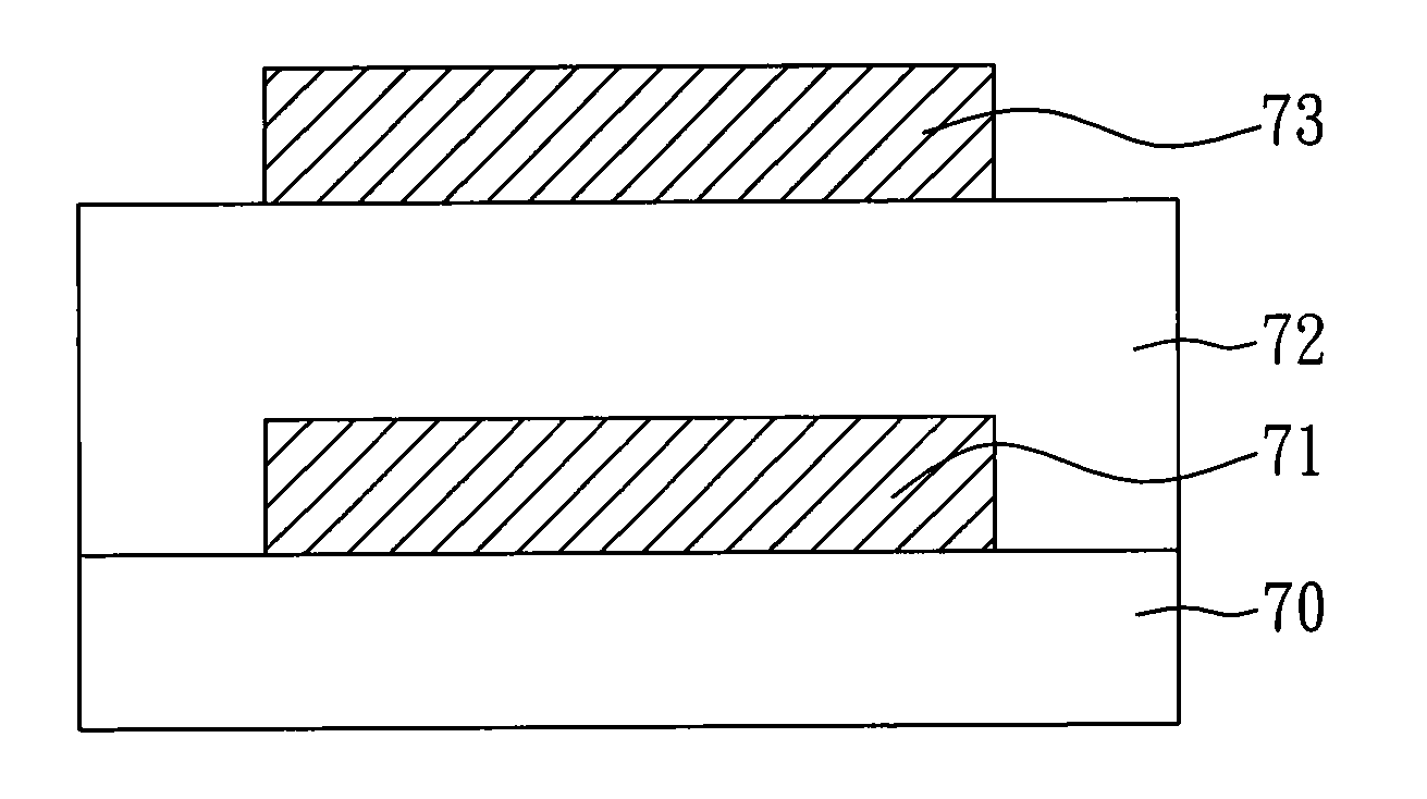
[0061]As shown in FIG. 7A, a substrate 70 was provided, and a first electrode 71 was formed on the substrate 70. In the present embodiment, the preparing method and the material of the first electrode 71 are the same as the process for forming the gate electrode illustrated in Embodiment 1. In the present embodiment, the substrate 70 was a plastic substrate, the material of the first electrode 71 was Au, and the thickness of the first electrode 71 was about 80 nm.

[0062]Next, the substrate 70 having the first electrode 71 formed thereon was dipped into the silk solution prepared in Embodiment 1 for 15 mins to coat the substrate 70 having the first electrode 71 with the silk solution. After the coating process, the substrate 70 coated with the silk solution was dried at 60° C. to form a silk film, and the silk film was used as an insulating layer 72, as shown in FIG. 7B.

[0063]Finally, the substrate 70 was placed into a vacuum chamber (not shown in the figure) with pressur...


PUM

PropertyMeasurementUnit
Nanoscale particle sizeaaaaaaaaaa
Tafel constantaaaaaaaaaa

Abstract

An electronic grade silk solution, an organic thin film transistor (OTFT) and a metal-insulator-metal capacitor with silk protein as the insulating material manufactured by use of the silk solution, and methods for manufacturing the same are disclosed. The OTFT of the present invention comprises: a substrate; a gate disposed on the substrate; a gate insulating layer containing silk protein, which is disposed on the substrate and covers the gate; an organic semiconductor layer; and a source and a drain, wherein the organic semiconductor layer, the source and the drain are disposed over the gate insulating layer.

Description

CROSS REFERENCE TO RELATED APPLICATION[0001]This application is a continuation-in-part application, and claims benefit of U.S. patent application Ser. No. 12 / 761,008, filed Apr. 15, 2010, entitled “OTFT AND MIM CAPACITOR USING SILK PROTEIN AS DIELECTRIC MATERIAL AND METHODS FOR MANUFACTURING THE SAME,” by Jenn-Chang Hwang, Chung Hwa Wang, and Chao Ying Hsieh, which status is pended, the disclosure of which is hereby incorporated herein in its entirety by reference.[0002]Some references, which may include patents, patent applications and various publications, are cited and discussed in the description of this invention. The citation and / or discussion of such references is provided merely to clarify the description of the present invention and is not an admission that any such reference is “prior art” to the invention described herein. All references cited and discussed in this specification are incorporated herein by reference in their entireties and to the same extent as if each ref...

Claims


Application Information

Patent Timeline
IPC IPC(8): H01L51/30C07K14/435B05D5/12H01L51/42H01G4/14
CPCB82Y10/00H01L28/40H01L51/0545H01L51/052H01L51/0093H10K85/761H10K10/471H10K10/466
Inventor HWANG, JENN-CHANGWANG, CHUNG HWAHSIEH, CHAO YING
Owner NATIONAL TSING HUA UNIVERSITY
Why Eureka
Try Eureka