

Thermosetting die bond film, dicing die bond film and semiconductor device
- Summary
- Abstract
- Description
- Claims
- Application Information
AI Technical Summary
Benefits of technology
Problems solved by technology
Method used
Image

Examples
example 1
[0146]An adhesive composition solution having a concentration of 23.6% by weight was obtained by dissolving the following (a) to (d) in methyl ethyl ketone.
[0147](a) 280 parts by weight of an epoxy resin (Epicoat 1004 manufactured by Japan Epoxy Resin Co., Ltd., melting point: 97° C.)
[0148](b) 306 parts by weight of a phenol resin (Milex XLC-4L manufactured by Mitsui Chemicals, Inc., melting point: 62° C.)
[0149](c) 100 parts by weight of an acrylic acid ester-based polymer having ethyl acrylate-methyl methacrylate as a main component (SG-708-6 manufactured by Nagase ChemteX Corporation, glass transition temperature: 6° C.)
[0150](d) 237 parts by weight of spherical silica (SO-25R manufactured by Admatechs Co., Ltd.)
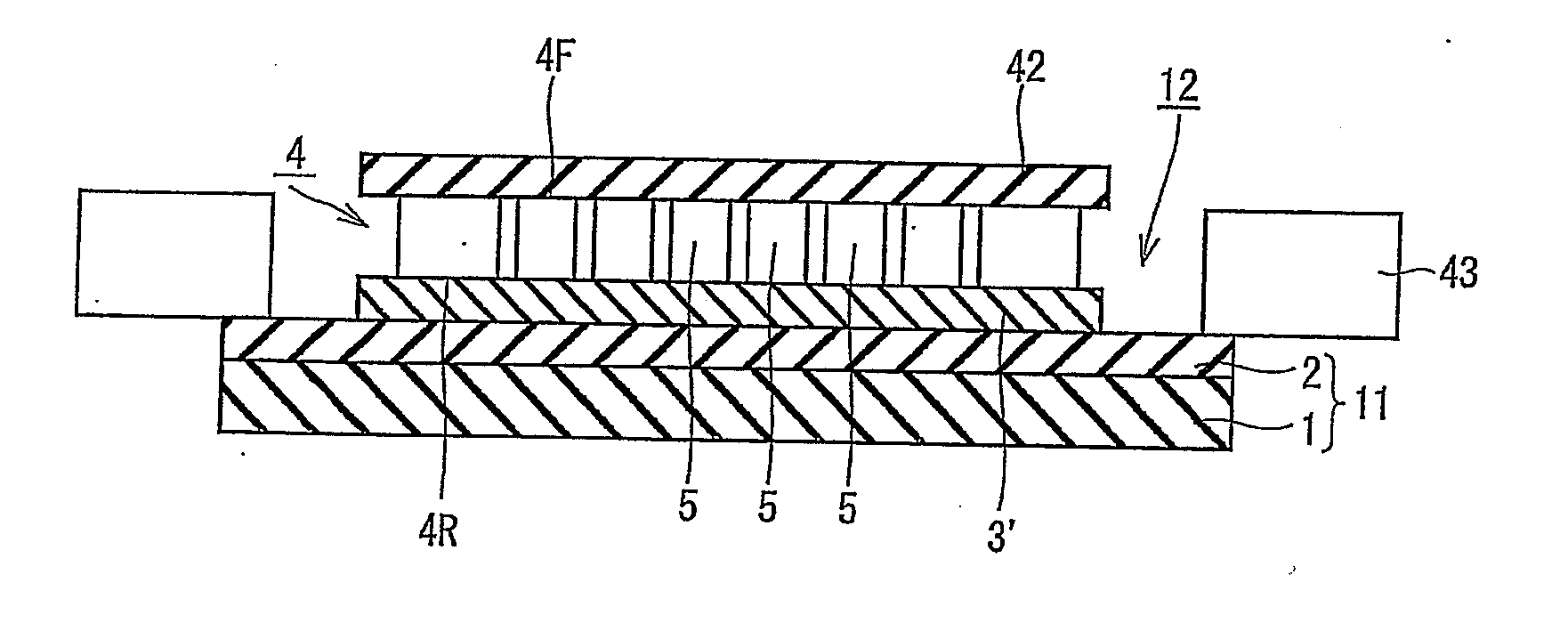
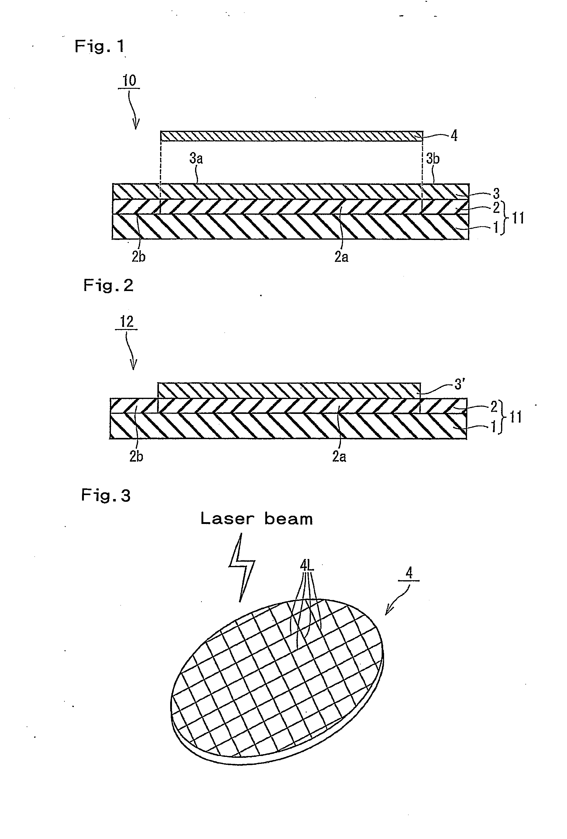
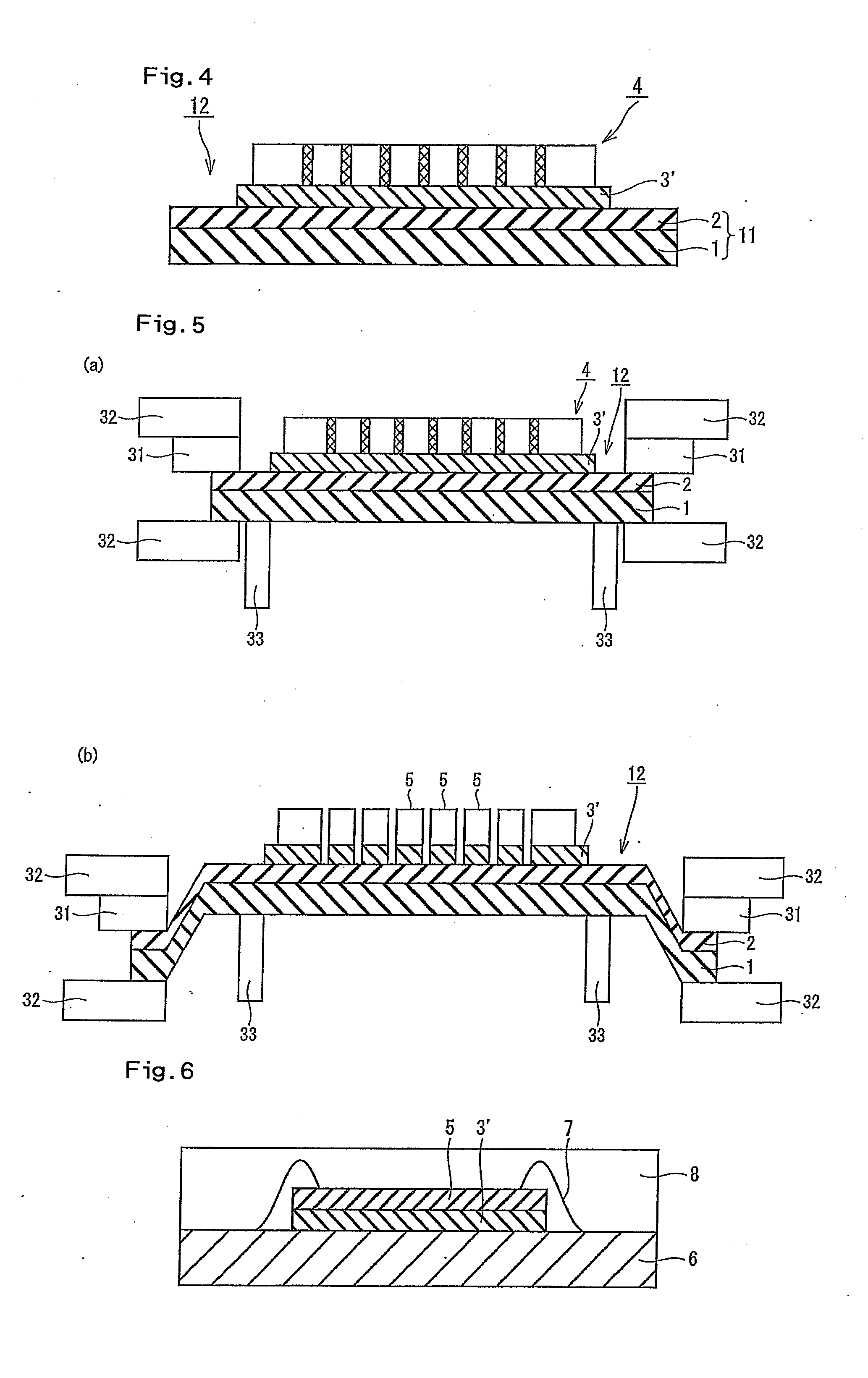
[0151]This adhesive composition solution was applied on a release-treated film (peel liner) composed of a 50 μm thick polyethylene terephthalate film subjected to a silicone release treatment and then dried at 130° C. for 2 minutes to produce a 25 μm thick die bond film A....
example 2
[0152]In Example 2, a die bond film B according to the present example was produced in the same manner as in Example 1 except that the added amount of the epoxy resin of (a) was changed to 270 parts by weight and the added amount of the phenol resin of (b) was changed to 296 parts by weight.
example 3
[0153]In Example 3, a die bond film C according to the present example was produced in the same manner as in Example 1 except that the added amount of the epoxy resin of (a) was changed to 113 parts by weight and the added amount of the phenol resin of (b) was changed to 121 parts by weight.
PUM
| Property | Measurement | Unit |
|---|---|---|
| Temperature | aaaaa | aaaaa |
| Temperature | aaaaa | aaaaa |
| Temperature | aaaaa | aaaaa |
Abstract
Description
Claims
Application Information