
Low cost solar cells formed using a chalcogenization rate modifier

a solar cell and chalcogenization rate technology, applied in the field of photovoltaic devices, to achieve the effects of increasing gallium exposure, accelerating gallium processing, and increasing surface area exposur

Inactive Publication Date: 2011-12-01
AERIS CAPITAL SUSTAINABLE IP
View PDF0 Cites 70 Cited by
  • Summary
  • Abstract
  • Description
  • Claims
  • Application Information

AI Technical Summary

Benefits of technology

[0012]For any of the embodiments herein, it is also possible to have two or more elements of IB elements in the chalcogenide particle and / or the resulting intermediate film and / or final absorber layer. One notable problem encountered when creating CIG(S)Se films for solar cells using low cost 2-step selenization methods is preventing Ga from segregating to the back of the film. Two-step selenization methods entail one step where a metal, oxide, or chalcogenide (or other Ag, Au, Cu, In, Ga, S, or Se containing compounds) precursor film is deposited, and then subsequently selenized (and / or sulfidized) in a second step. The approach described herein is to create (Ag,Cu)(In,Ga)(Se,S)2 (hereafter referred to as ACIGS) by adding Ag to the precursor film. It has been found that this enables more of the Ga to remain forward in the film. Ga at the front surface of the film allows for higher open-circuit voltage solar cells and therefore higher efficiencies.
[0015]An additional benefit of controlling the chalcogenization reaction rate is that it allows for the optimization of the rate of crystallization to achieve good crystal quality with as fast a rate as possible (to reduce the associated manufacturing costs). It is common knowledge that crystals which are grown too fast can have poor quality, specifically in the form of small grains and many point defects, due to insufficient time for grain growth and the atoms forming the growing crystal not having enough time to find the appropriate positions in the lattice. On the other hand, if crystallization occurs very slowly, then the material becomes costly to manufacture. A crystallization rate modifier is useful to slow down reactions that occur too quickly to create high quality crystals, or speed up reactions that occur too slowly to be cost effective in production. In embodiments of the present invention, the chalcogenization rate modifier is compound selective, such that it promotes the preferential chalcogenization of one species over another in the crystal growth.
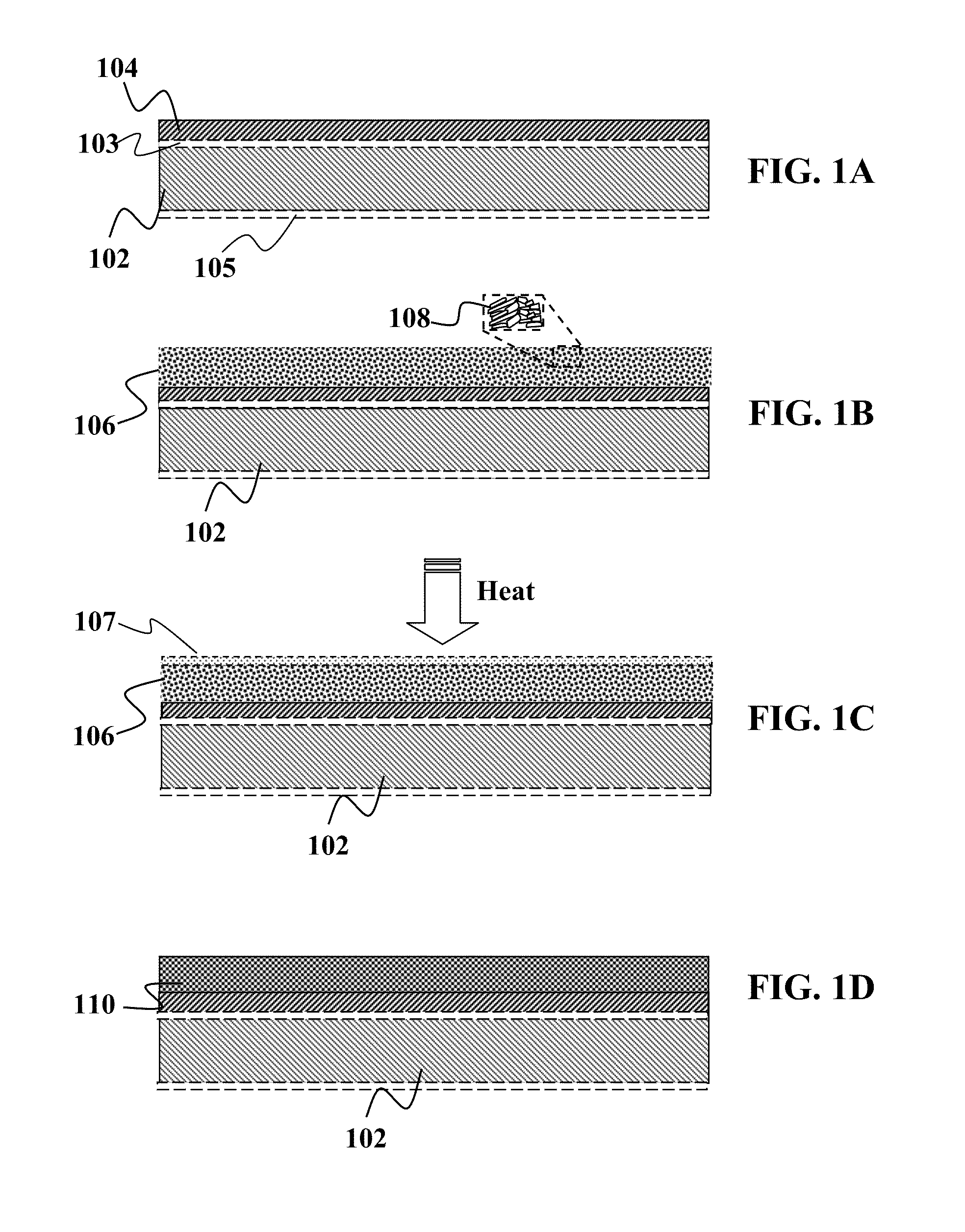
[0019]For any of the embodiments herein, the embodiments can be configured to incorporate one or more of the following. For example, upper surfaces of the areas of copper-gallium alloy phase are exposed in the densified layer to increase surface area exposure of copper-gallium alloy phase during group VIA processing. Optionally, some embodiments can minimize the amount of copper-indium present in the densified layer. Optionally, the method includes limiting availability of free, elemental indium in the densified layer by binding the chalcogenization rate modifier to form a non-copper, Group IB-indium alloy phase. Optionally, the non-copper, Group IB-indium alloy phase comprises Au—In. Optionally, the non-copper, Group IB-indium alloy phase comprises Ag—In.
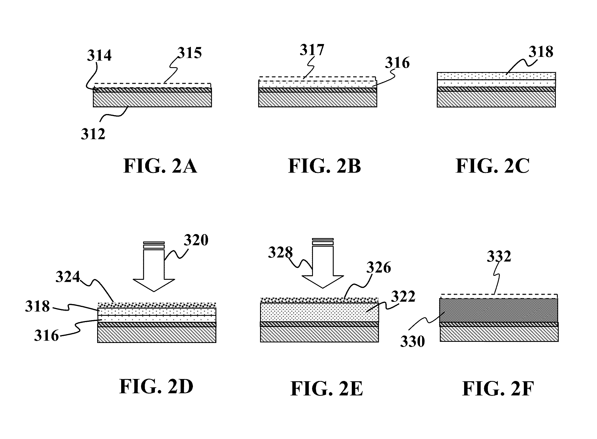
[0021]For any of the embodiments herein, the embodiments can be configured to incorporate one or more of the following. For example, the chalcogenization rate modifier is selective for gallium. Without being tied to any particular theory, some embodiments may speed up gallium processing. Some may increase gallium exposure by causing greater surface area exposure of IB-IIIA areas on the densified film. Optionally, the chalcogenization rate modifier is selective for indium. Without being tied to any particular theory, some embodiments may delay indium processing by decreasing the amount of copper-IIIA or copper-indium in the densified film. Some embodiments completely remove all copper indium in the densified layer. Some embodiments may leave 10 wt % or less of what would have been there without the rate modifier. Optionally, the process gas atmosphere involves using a selenium atmosphere. Optionally, processing involves using a selenium-based atmosphere and then a sulfur-based atmosphere. Optionally, processing involves using a selenium-based atmosphere and a sulfur-based atmosphere. Optionally, chalcogenization rate modifier forms a silver-group IIIA alloy phase in the densified layer. Optionally, chalcogenization rate modifier forms a gold-group IIIA alloy phase in the densified layer. Optionally, the method involves limiting availability of free, elemental indium in the densified layer by binding the chalcogenization rate modifier to form a silver-IIIA alloy phase. Optionally, the chalcogenization rate modifier alloy phase is formed in localized areas in a repeating or other pattern in the densified layer. Optionally, the chalcogenization rate modifier alloy phase is concentrated in islands of material in the densified layer. Optionally, the densified layer includes chalcogenization rate modifier-indium phase and areas of IB-gallium alloy phase in distributed patterns over the substrate. Optionally, heating the precursor creates segregated chalcogenization rate modifier-indium phase and areas of IB-gallium alloy phase over the substrate.

Problems solved by technology

One notable problem encountered when creating CIG(S)Se films for solar cells using low cost 2-step selenization methods is preventing Ga from segregating to the back of the film.

Method used


Image

  • Low cost solar cells formed using a chalcogenization rate modifier
  • Low cost solar cells formed using a chalcogenization rate modifier
  • Low cost solar cells formed using a chalcogenization rate modifier

Examples


embodiment 1

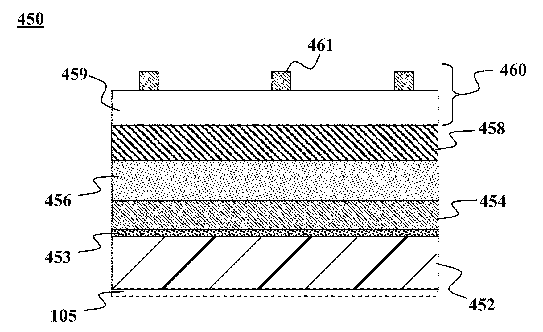
[0050]A metal foil substrate was sputtered with Mo to form a 500 nm to 1000 nm Mo film to serve as the back contact. A barrier layer of 50 nm to 300 nm of Chromium, TiN, HfN, or other transition metal nitride barrier was formed onto the Mo back contact. A precursor ink comprised of Cu, In, Ga, and Ag, and atomic ratios Ag / (Ag+Cu)=0.1-0.3, Ga / (Ga+In)=0.35-0.5, and (Ag+Cu) / (Ga+In)=0.80-1.0. For the present embodiment, an approximately 0.5-2.5 micron thick layer of the precursor material containing solution is deposited on the substrate. The precursor material may be dispersed in a solvent such as water, alcohol or ethylene glycol with the aid of organic surfactants and / or dispersing agents described herein to form an ink.

[0051]The precursor layer is annealed with a ramp-rate of 1-5° C. / sec, preferably over 5° C. / sec, to a temperature of about 225° to about 575° C. preferably for about 30 seconds to about 600 seconds to enhance densification and / or alloying between Cu, In, and Ga in an...

embodiment 2

[0055]A metal foil substrate was sputtered with Mo to form a 500 nm to 1000 nm Mo film to serve as the back contact. A barrier layer of 50 nm to 300 nm of Chromium, TiN, HfN, or other transition metal nitride barrier was formed onto the Mo back contact. A precursor ink comprised of Cu, In, Ga, and Ag, and atomic ratios Ag / (Ag+Cu)=0.2-0.3, Ga / (Ga+In)=0.3-0.4, and (Ag+Cu) / (Ga+In)=0.8-0.9. For the present embodiment, an approximately 0.5-2.5 micron thick layer of the precursor material containing solution is deposited on the substrate. The precursor material may be dispersed in a solvent such as water, alcohol or ethylene glycol with the aid of organic surfactants and / or dispersing agents described herein to form an ink.

[0056]The precursor layer is annealed with a ramp-rate of 1-5° C. / sec, preferably over 5° C. / sec, to a temperature of about 225° to about 575° C. preferably for about 30 seconds to about 600 seconds to enhance densification and / or alloying between Cu, In, and Ga in an a...

embodiment 3

[0060]A metal foil substrate was sputtered with Mo to form a 500 nm to 1000 nm Mo film to serve as the back contact. A barrier layer of 50 nm to 300 nm of Chromium, TiN, HfN, or other transition metal nitride barrier was formed onto the Mo back contact. The method may be used to form a IB-IIB-IVA-VIA absorber material. A precursor ink is provided wherein Ag / IB=0.1-0.4. A method of forming (Ag,Cu)xZnySnz, (Ag,Cu)xZnySnzSa (ACZTS), (Ag,Cu)xZnySnzSeb (ACZTSe) or (Ag,Cu)xZnySn2SaSeb (ACZTSSe) layers with well-defined total bulk stoichiometries, wherein x ranges from 1.5 to 2.5, y ranges from 0.9 to 1.5, z ranges from 0.5 to 1.1, a ranges from 0 to 4.2, preferably from 0.1 to 4.2, and b ranges from 0 to 4.2, preferably from 0.1 to 4.2, and which method is easy to apply and suitable for large scale production of thin film solar cells.

[0061]In one embodiment, the stoichiometric ratio for a ACZTS solar cell precursor foil may be (Ag: 10 at.-%, Cu: 40 at.-%, Zn: 25 at.-%, Sn: 25 at.-%) Optio...


PUM


Abstract

Methods and devices are provided for forming an absorber layer. In one embodiment, a method is provided comprising of depositing a precursor material onto a substrate, wherein the precursor material may include or may be used with an additive to minimize concentration of group IIIA material such as Ga in the back portion of the final semiconductor layer. The additive may be a non-copper Group IB additive in elemental or alloy form.

Description

CROSS-REFERENCE TO RELATED APPLICATIONS[0001]This application claims priority to U.S. Provisional Application Ser. No. 61 / 290,490 filed Dec. 28, 2009 and fully incorporated herein by reference for all purposes.FIELD OF THE INVENTION[0002]This invention relates generally to photovoltaic devices, and more specifically, to use of additives or dopants during photovoltaic device manufacturing for enhanced bandgap grading.BACKGROUND OF THE INVENTION[0003]Solar cells and solar modules convert sunlight into electricity. These electronic devices have been traditionally fabricated using silicon (Si) as a light-absorbing, semiconducting material in a relatively expensive production process. To make solar cells more economically viable, solar cell device architectures have been developed that can inexpensively make use of thin-film, preferably non-silicon, light-absorbing semiconductor materials such as but not limited to copper-indium-gallium-selenide (CIGS).[0004]Many traditional thin-film CI...

Claims


Application Information

Patent Timeline
IPC IPC(8): H01L31/0264
CPCY02E10/541H01L31/0322H01L21/02568H01L21/02601H01L21/02614H01L21/02628Y02P70/50
Inventor JACKREL, DAVID B.DICKEY, KATHERINEWOODRUFF, JACOB
Owner AERIS CAPITAL SUSTAINABLE IP
Learn More