Semiconductor device and method of fabricating the same

a semiconductor field effect transistor and semiconductor technology, applied in the direction of semiconductor devices, electrical equipment, transistors, etc., can solve the problems of voltage drop across a polysilicon gate, decrease of threshold voltage of mosfet, and degradation of properties, so as to facilitate epitaxial growth and improve channel performance , the effect of high quality

Active Publication Date: 2011-12-15
INST OF MICROELECTRONICS CHINESE ACAD OF SCI
View PDF3 Cites 17 Cited by
  • Summary
  • Abstract
  • Description
  • Claims
  • Application Information

AI Technical Summary

Benefits of technology

[0008]One object of the present invention is to provide an MOSFET having an increased output current, an increased operating speed and a reduced power consumption, and a method for manufacturing the same.
[0017]In the semiconductor device of the present invention, the slant sidewall of the second semiconductor layer facilitates the epitaxial growth of the first semiconductor layer. Consequently, the first semiconductor layer is of high quality and improves performance of the channel region of the semiconductor device. The first semiconductor layer is made of a high-mobility material, which leads to an increased output current, an increased operation frequency and a reduced power consumption when the first semiconductor layer is used as the channel region. The most suitable materials can be used for the source / drain regions and the channel regions to provide optimal performance respectively.
[0018]In a preferred embodiment, the first semiconductor layer is an epitaxial layer which has a top surface and a bottom surface matching {100} plane of Si, and a sidewall in contact with the second semiconductor layer and matching {111} plane of Si. The interface (i. e. sidewall) between the first semiconductor layer and the second semiconductor layer substantially preserves integrity and continuity of a crystal structure, which decreases an amount of defects due to the existence of the interface. The epitaxial growth in this direction can provide a flat surface, which ensures a uniform thickness of the channel region.
[0019]In the method of the present invention, a doping process for providing the source / drain regions is performed before formation of the channel region, which avoids a diffusion of dopants towards the channel region and thus decreases an amount of defects in the channel region and improves greatly the performance of the semiconductor device.

Problems solved by technology

However, due to the reduced gate length, the gate has a poor controllability on a channel region, which degrades properties of the MOSFET, especially causes a short channel effect in which a threshold voltage of the MOSFET decreases.
Moreover, a poor conductivity of polysilicon causes a voltage drop across a polysilicon gate when a voltage is applied to the gate.
However, the above novel devices, such as the dual-gate device, the ultra-thin SOI device, and the MOS device having a metal gate, still use conventional channel materials, which limits maximum values of an output current and an operating frequency, and has no improvement in a power consumption.

Method used


Image

  • Semiconductor device and method of fabricating the same
  • Semiconductor device and method of fabricating the same
  • Semiconductor device and method of fabricating the same

Examples


Embodiment Construction

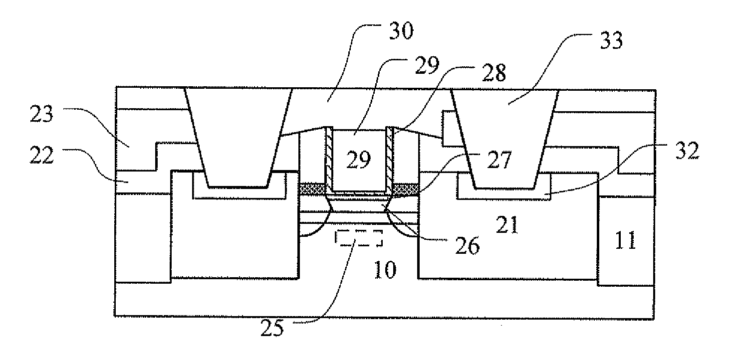
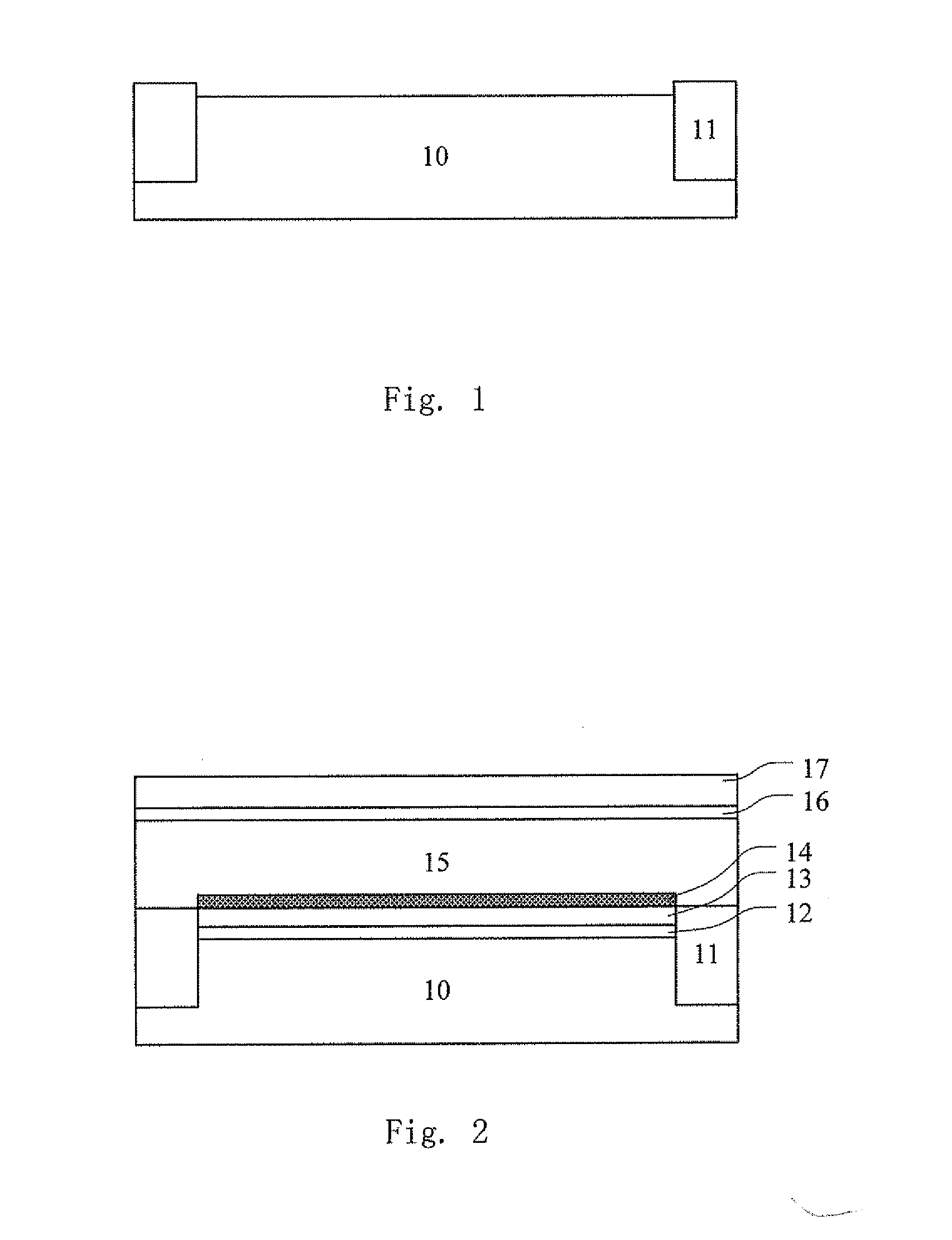
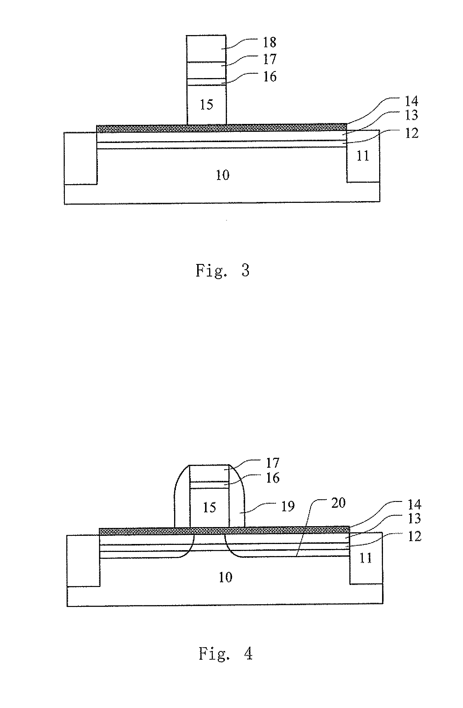
[0021]Exemplary embodiments of the present invention are described in more details below with reference to the accompanying drawings. In the drawings, like reference numerals denote like members. The figures are not drawn to scale, for the sake of clarity.

[0022]It should be understood that when one layer or region is referred to as being “above” or “on” another layer or region in the description of device structure, it can be directly above or on the other layer or region, or other layers or regions may be intervened therebetween. Moreover, if the device in the figures is turned over, the layer or region will be “under” or “below” the other layer or region.

[0023]In contrast, when one layer is referred to as being “directly on” or “on and adjacent to” another layer or region, there are not intervening layers or regions present.

[0024]Some particular details of the invention will be described, such as an exemplary structure, material, dimension, process step and fabricating method of t...


PUM


Abstract

The present application discloses a semiconductor device and a method for manufacturing the same. The semiconductor device comprises a semiconductor substrate; a first semiconductor layer on the semiconductor substrate; a second semiconductor layer surrounding the first semiconductor layer; a high k dielectric layer and a gate conductor formed on the first semiconductor layer; source / drain regions formed in the second semiconductor layer, wherein the second semiconductor layer has a slant sidewall in contact with the first semiconductor layer. The semiconductor device has an increased output current, an increased operating speed, and a reduced power consumption due to the channel region of high mobility.

Description

BACKGROUND OF THE INVENTION[0001]1. Field of Invention[0002]The present invention relates generally to a semiconductor device and a method for manufacturing the same, and more particularly, to an MOSFET (metal oxide semiconductor field effect transistor) structure with a channel region of high mobility and a method for manufacturing the same.[0003]2. Description of Prior Art[0004]One trend of the integrated circuit technology is to integrate as many MOSFETs as possible in a unit area of a chip. With scaling down of the MOSFET dimensions, a gate length is reduced to less than 32 nm. However, due to the reduced gate length, the gate has a poor controllability on a channel region, which degrades properties of the MOSFET, especially causes a short channel effect in which a threshold voltage of the MOSFET decreases. Moreover, a poor conductivity of polysilicon causes a voltage drop across a polysilicon gate when a voltage is applied to the gate. Thus, an actual gate voltage applied to th...

Claims


Application Information

Patent Timeline
Patent Type & Authority Applications(United States)
IPC IPC(8): H01L29/772H01L21/336
CPCH01L29/4966H01L29/66545H01L29/66636H01L29/6659H01L29/1083H01L29/045H01L29/7834H01L29/105H01L29/517H01L29/66651H01L29/165H01L29/495H01L29/1054H01L29/665H01L29/6653
Inventor ZHU, HUILONGLIANG, QINGQINGLUO, ZHIJIONGYIN, HAIZHOU
Owner INST OF MICROELECTRONICS CHINESE ACAD OF SCI
Why Eureka
Try Eureka