Storage element, method for manufacturing storage element, and memory

a storage element and manufacturing method technology, applied in the field of storage elements, can solve the problems of lowering resistance, difficulty in operation without application, and lowering the quality of the tunnel barrier layer, and achieve the effect of reducing power consumption, reducing resistance, and sufficient flatness

Active Publication Date: 2011-12-29
SONY CORP
View PDF1 Cites 23 Cited by
  • Summary
  • Abstract
  • Description
  • Claims
  • Application Information

AI Technical Summary

Benefits of technology

[0022]In the method for manufacturing a storage element according to this embodiment of the present disclosure, in the step of forming the tunnel barrier layer, the tunnel barrier layer is formed to a predetermined thickness in such a manner that the step is divided into at least two steps in forming the whole tunnel barrier layer. By thus carrying out the forming step of the tunnel barrier layer in at least two steps ...

Problems solved by technology

However, the following problems exist in lowering the resistance by decreasing the thickness of the MgO tunnel barrier layer.
(2) The quality of the tunnel barrier layer ...

Method used


Image

  • Storage element, method for manufacturing storage element, and memory
  • Storage element, method for manufacturing storage element, and memory
  • Storage element, method for manufacturing storage element, and memory

Examples


first embodiment

1. First Embodiment of the Present Disclosure

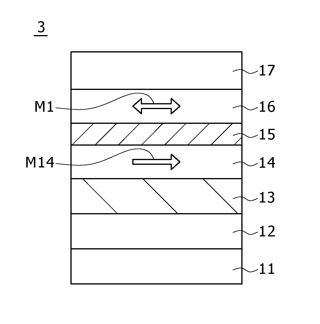
Configuration Example of Memory

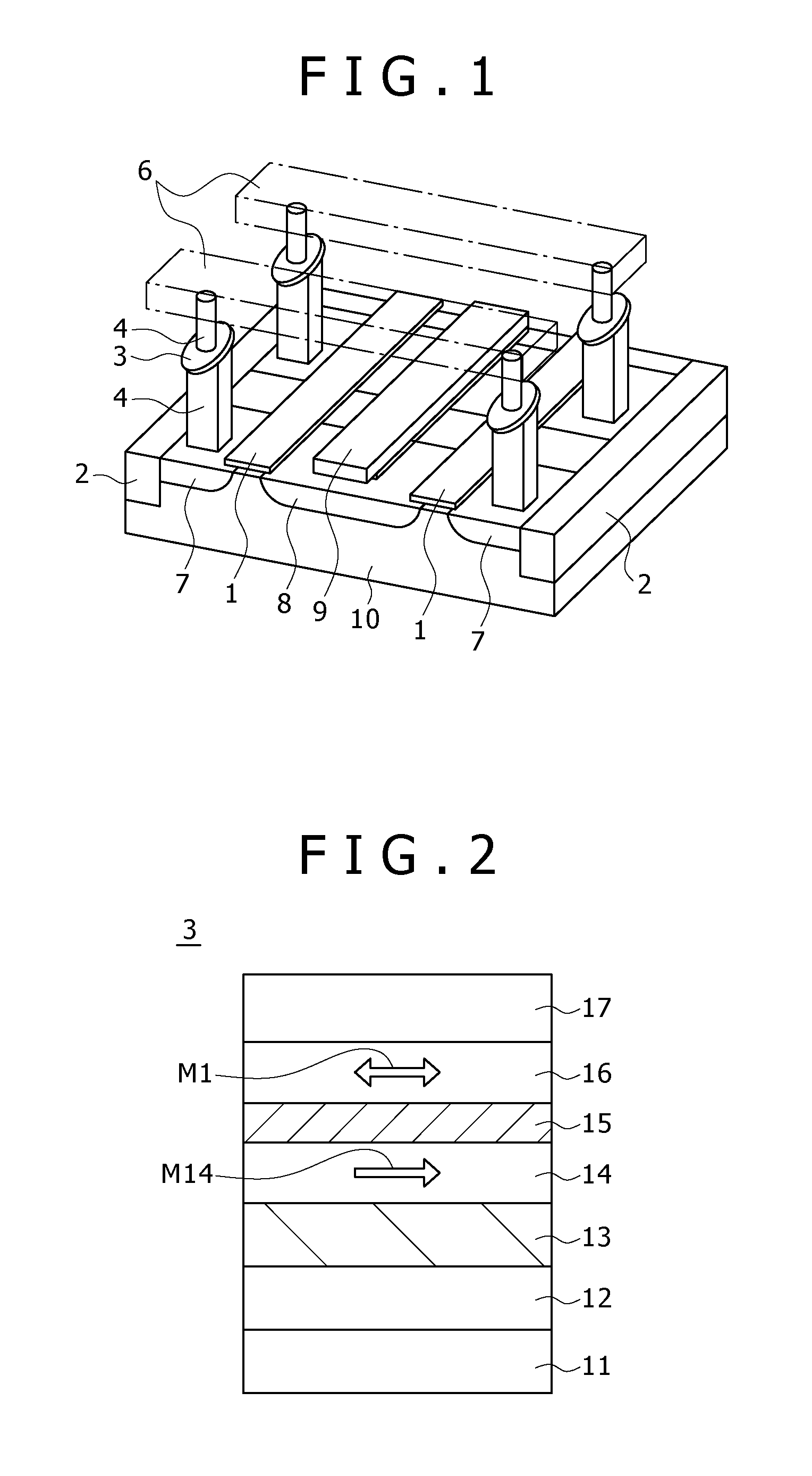
[0038]FIG. 1 is a schematic configuration diagram (perspective view) of a memory according to a first embodiment of the present disclosure.

[0039]This memory is formed by disposing storage elements capable of retaining information based on the magnetization state near the intersections of two kinds of address interconnects (e.g. word line and bit line) orthogonal to each other.

[0040]Specifically, in part isolated by an element isolating layer 2 in a semiconductor substrate 10 such as a silicon substrate, a drain region 8, a source region 7, and a gate electrode 1 are formed as a selection transistor for selecting the corresponding memory cell. The gate electrode 1 serves also as one address interconnect (e.g. word line) extended along the anteroposterior direction in the diagram.

[0041]The drain region 8 is formed in common to the selection transistors on the left and right sides in the diagram. An interconnec...

experimental example 1

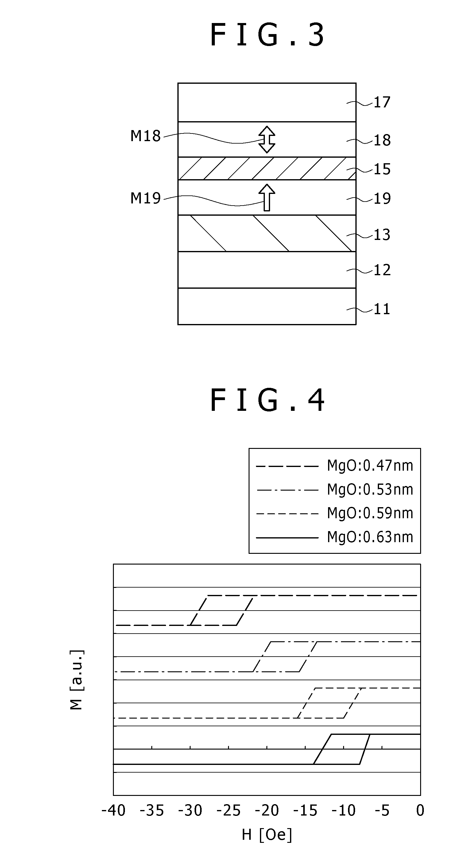
[0084]A 5-nm-thick Ta layer was formed as the base layer 12 on a silicon substrate with a thermally-oxidized film. Next, a 20-nm-thick PtMn layer was formed as the antiferromagnetic layer 13, and 2-nm-thick CoFe / 0.8-nm-thick Ru / 2-nm-thick CoFeB layers were sequentially formed as the magnetization pinned layer 14. In this example, a spin valve structure made by utilizing the antiferromagnetic layer 13 was used, and a synthetic ferrimagnetic structure made with the intermediary of Ru was used as the structure of the magnetization pinned layer 14.

[0085]Next, as the tunnel barrier layer, a 0.4-nm-thick MgO layer was formed in a first step and then a 0.07-nm-thick MgO layer for the remaining thickness was formed in a second step. At last, a 3-nm-thick CoFeB layer as the free magnetization layer and a cap layer were sequentially formed. After the multilayer body having the above-described configuration was formed, magnetic field heat treatment was performed at 320° C. Through the above-de...

experimental examples 2 to 4

[0086]MTJ elements of experimental examples 2 to 4 were fabricated by the same method as that of experimental example 1 except for that the thickness of the MgO layer formed in the second step for forming the tunnel barrier layer was set to 0.13 nm, 0.19 nm, and 0.23 nm, respectively. In the MTJ elements of experimental examples 2 to 4, the thicknesses of the tunnel barrier layer were 0.53 nm (experimental example 2), 0.59 nm (experimental example 3), and 0.63 nm (experimental example 4).

(Comparison of Magnetization Curve)

[0087]FIG. 4 shows magnetization curves of the storage layer about the respective fabricated samples of the MTJ elements of experimental examples 1 to 4. In FIG. 4, the abscissa indicates the applied magnetic field H [Oe] and the ordinate indicates the magnetization M [a. u].

[0088]The elements of experimental examples 1 to 4 exhibited favorable squareness attributed to planarization of the tunnel barrier layer.

[0089]In experimental example 4, in which the thickness...


PUM


Abstract

Disclosed herein is a storage element, including: a storage layer configured to retain information based on a magnetization state of a magnetic material; and a magnetization pinned layer configured to be provided for the storage layer with intermediary of a tunnel barrier layer, wherein the tunnel barrier layer has a thickness not less than or equal to 0.1 nm to not more than or equal to 0.6 nm and interface roughness less than 0.5 nm, and information is stored in the storage layer through change in direction of magnetization of the storage layer by applying a current in a stacking direction and injecting a spin-polarized electron.

Description

BACKGROUND[0001]The present disclosure relates to a storage element with a configuration that has perpendicular magnetic anisotropy with respect to the film plane and obtains magnetoresistance change through perpendicular current application, a method for manufacturing a storage element, and a memory including this storage element.[0002]Along with dramatic development of various kinds of information apparatus ranging from high-capacity servers to mobile terminals, further enhancement in the performance, such as increases in the degree of integration and the speed and power consumption reduction, is pursued also regarding elements such as memory and logic that configure the information apparatus. In particular, the advance of the semiconductor non-volatile memory is significant and the spread of the flash memory as a large-size file memory is progressing at such a rapid pace as to drive out the hard disk drive. On the other hand, in anticipation of expansion into the code storage and...

Claims


Application Information

Patent Timeline
IPC IPC(8): H01L29/82H01L43/12
CPCB82Y25/00B82Y40/00G11C11/16H01F10/3254H01L43/12H01F10/3286H01F10/329H01F41/307H01L43/08H01F10/3263G11C11/1675G11C11/161H10N50/01H10N50/10H10B61/22
Inventor UCHIDA, HIROYUKIHOSOMI, MASANORIOHMORI, HIROYUKIBESSHO, KAZUHIROHIGO, YUTAKAYAMANE, KAZUTAKA
Owner SONY CORP
Why Eureka
Try Eureka