This helps you quickly interpret patents by identifying the three key elements:
Problems solved by technology
Method used
Benefits of technology
Benefits of technology
[0007]In view of the above problem, an object is to provide a semiconductor device including an oxide semiconductor, which has stable electrical characteristics and improved reliability.
[0008]In one embodiment of the disclosed invention, insulating films each including a material containing a Group 13 element and oxygen are formed in contact with an oxide semiconductor film, whereby the interfaces with the oxide semiconductor film can be kept in a favorable state. Further, the insulating films each include a region where the proportion of oxygen is higher than that in the stoichiometric composition, so that oxygen is supplied to the oxide semiconductor film; thus, oxygen defects in the oxide semiconductor film can be reduced. Furthermore, the insulating films in contact with the oxide semiconductor film each have a stacked structure so that films each containing aluminum are provided over and under the oxide semiconductor film, whereby entry of water into the oxide semiconductor film can be prevented. Specifically, structures described below can be employed, for example.
[0017]According to one embodiment of the present invention, a transistor having stable electrical characteristics is provided.
[0018]Further, according to one embodiment of the present invention, a semiconductor device which includes a transistor having excellent electrical characteristics and high reliability can be provided.
Problems solved by technology
However, electrical conductivity of the oxide semiconductor may potentially change in the following case: the oxide semiconductor has deviation from the stoichiometric composition because of oxygen vacancy; a factor such as hydrogen or water causing formation of an electron donor enters the oxide semiconductor in a manufacturing process of a device; or the like.
Method used
Image
Click on the blue label to locate the original text in one second.
Reading with bidirectional positioning of images and text.
Examples
embodiment 1
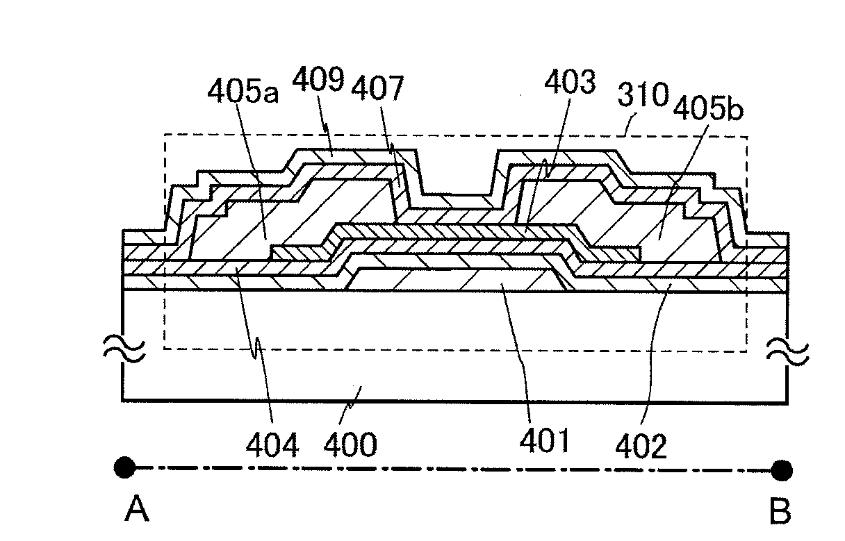
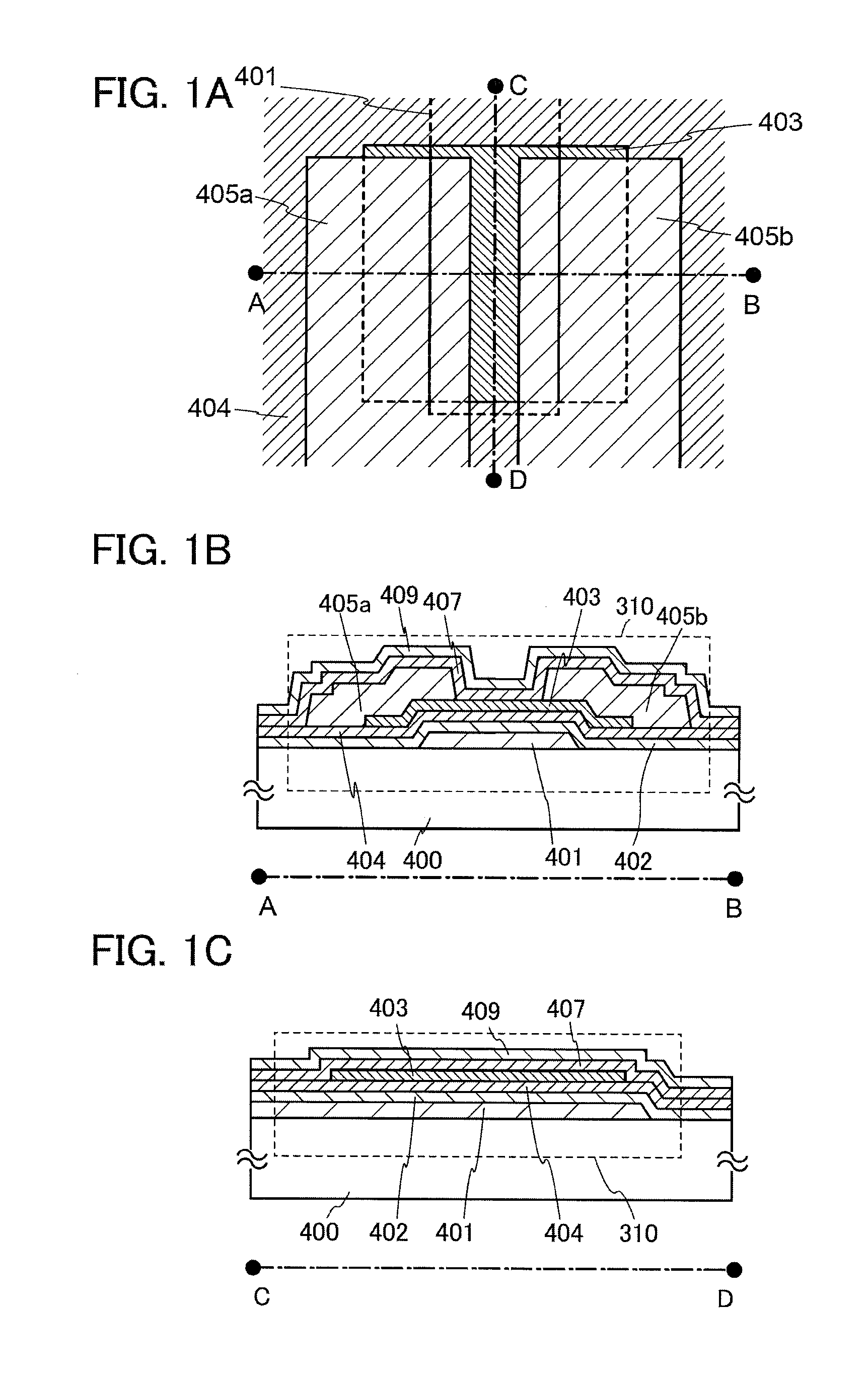
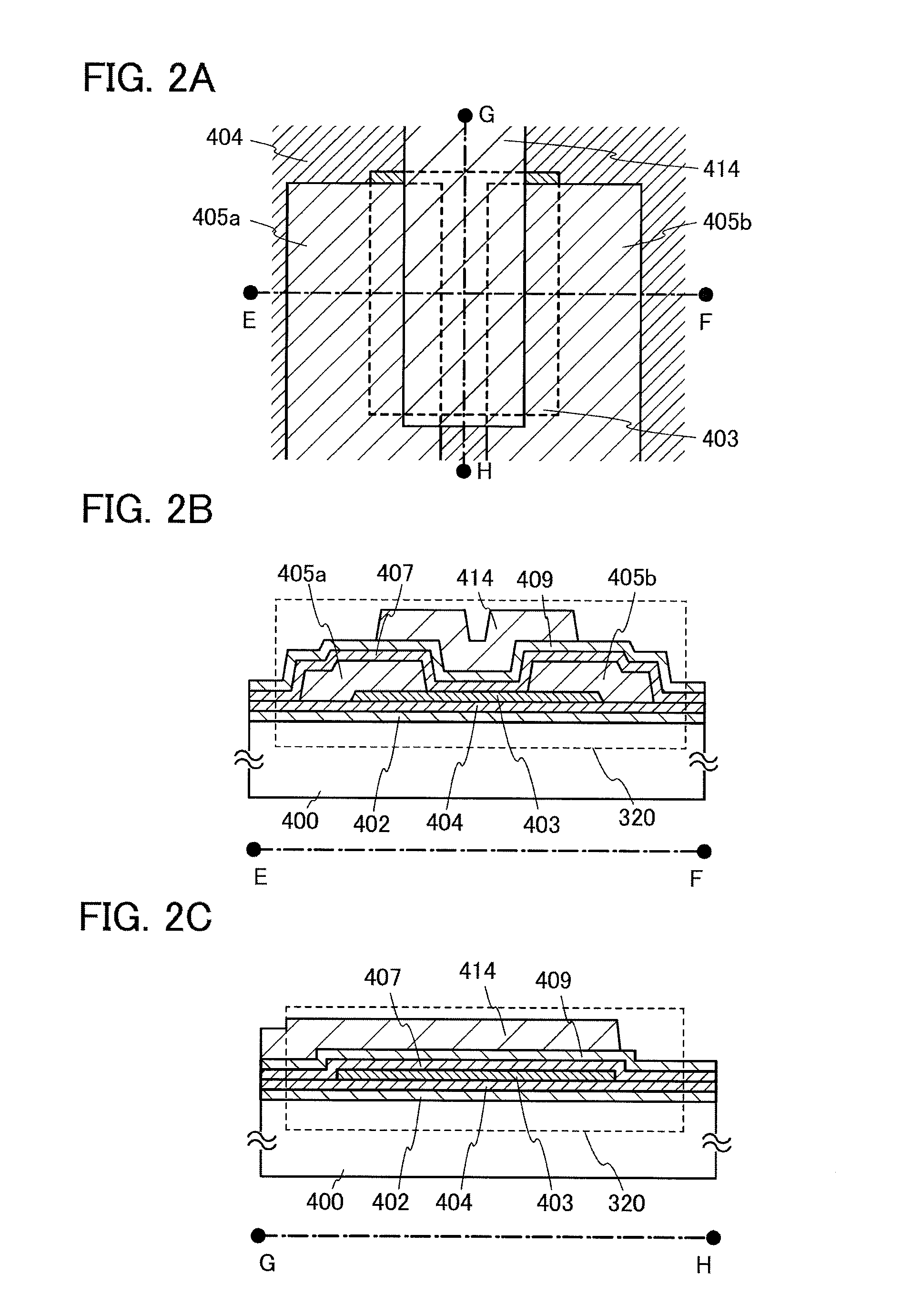
[0035]In this embodiment, one embodiment of a semiconductor device and a method for manufacturing the semiconductor device will be described with reference to FIGS. 1A to 1C, FIGS. 2A to 2C, FIGS. 3A to 3C, FIGS. 4A to 4F, FIGS. 5A to 5E, and FIGS. 6A to 6E.
[0036]FIGS. 1A to 1C are a plan view and cross-sectional views of a transistor 310 as an example of a semiconductor device according to one embodiment of the disclosed invention. In FIGS. 1A to 1C, a bottom-gate transistor is illustrated as a transistor according to one embodiment of the disclosed invention. Here, FIG. 1A is a plan view and FIGS. 1B and 1C are cross-sectional views taken along line A-B and line C-D, respectively, of FIG. 1A. Note that part of components of the transistor 310 (e.g., a third metal oxide film 407, a fourth metal oxide film 409, and the like) is omitted in FIG. 1A for brevity.
[0037]The transistor 310 in FIGS. 1A to 1C includes, over a substrate 400 having an insulating surface, a gate electrode 401, ...
embodiment 2
[0144]A semiconductor device (also referred to as a display device) with a display function can be manufactured using the transistor an example of which is described in Embodiment 1. Moreover, some or all of the driver circuits which include the transistors can be formed over a substrate where the pixel portion is formed, whereby a system-on-panel can be obtained.
[0145]In FIG. 7A, a sealant 4005 is provided so as to surround a pixel portion 4002 provided over a first substrate 4001, and the pixel portion 4002 is sealed between the first substrate 4001 and a second substrate 4006. In FIG. 7A, a signalline driver circuit 4003 and a scan linedriver circuit 4004 which are formed using a single crystal semiconductor film or a polycrystalline semiconductor film over a substrate separately prepared are mounted over the first substrate 4001, in a region that is different from the region surrounded by the sealant 4005. Various signals and potential are supplied to the signalline driver ci...
embodiment 3
[0228]A semiconductor device disclosed in this specification can be applied to a variety of electronic devices (including game machines). Examples of electronic devices are a television set (also referred to as a television or a television receiver), a monitor of a computer or the like, a camera such as a digital camera or a digital video camera, a digital photo frame, a mobile phonehandset (also referred to as a mobile phone or a mobile phone device), a portable game machine, a portable information terminal, an audio reproducing device, a large-sized game machine such as a pachinko machine, and the like. Examples of electronic devices each including the liquid crystaldisplay device described in the above embodiment are described.
[0229]FIG. 11A illustrates a laptoppersonal computer, which includes a main body 3001, a housing 3002, a display portion 3003, a keyboard 3004, and the like. By applying the semiconductor device described in Embodiment 1 or 2, the laptop personal compute...
PUM
Abstract
An object is to provide a semiconductor device including an oxidesemiconductor, which has stable electrical characteristics and improved reliability. In a transistor including an oxidesemiconductor film, insulating films each including a material containing a Group 13 element and oxygen are formed in contact with the oxide semiconductor film, whereby the interfaces with the oxide semiconductor film can be kept in a favorable state. Further, the insulating films each include a region where the proportion of oxygen is higher than that in the stoichiometric composition, so that oxygen is supplied to the oxide semiconductor film; thus, oxygen defects in the oxide semiconductor film can be reduced. Furthermore, the insulating films in contact with the oxide semiconductor film each have a stacked structure so that films each containing aluminum are provided over and under the oxide semiconductor film, whereby entry of water into the oxide semiconductor film can be prevented.
Description
TECHNICAL FIELD[0001]The present invention relates to a semiconductor device and a method for manufacturing the semiconductor device.[0002]In this specification, a semiconductor device generally means a device which operates by utilizing semiconductor characteristics, and an electrooptic device, a semiconductor circuit, and electronic equipment are all semiconductor devices.BACKGROUND ART[0003]A technique by which transistors are formed using semiconductor thin films over a substrate having an insulating surface has been attracting attention. The transistor is applied to a wide range of electronic devices such as an integrated circuit (IC) and an image display device (display device). A silicon-based semiconductor material is widely known as a material for a semiconductor thin film applicable to a transistor. As another material, an oxide semiconductor has been attracting attention.[0004]For example, a transistor whose active layer uses an amorphous oxide containing indium (In), gal...
Claims
Application Information
Patent Timeline
Application Date:The date an application was filed.
Publication Date:The date a patent or application was officially published.
First Publication Date:The earliest publication date of a patent with the same application number.
Issue Date:Publication date of the patent grant document.
PCT Entry Date:The Entry date of PCT National Phase.
Estimated Expiry Date:The statutory expiry date of a patent right according to the Patent Law, and it is the longest term of protection that the patent right can achieve without the termination of the patent right due to other reasons(Term extension factor has been taken into account ).
Invalid Date:Actual expiry date is based on effective date or publication date of legal transaction data of invalid patent.

