

Nitride semiconductor light-emitting element and process for production thereof
a technology of light-emitting elements and semiconductors, which is applied in the direction of semiconductor devices, basic electric elements, electrical devices, etc., can solve the problems of increasing power dissipation, reducing the internal quantum yield, and reducing the luminous efficacy of leds, so as to improve the current-voltage characteristic, improve the efficiency of light-emitting elements, and improve the effect of current-voltage characteristics
- Summary
- Abstract
- Description
- Claims
- Application Information
AI Technical Summary
Benefits of technology
Problems solved by technology
Method used
Image

Examples
embodiments
[0066]Hereinafter, embodiments of a nitride-based semiconductor light-emitting device of the present invention will be described with reference to the drawings.
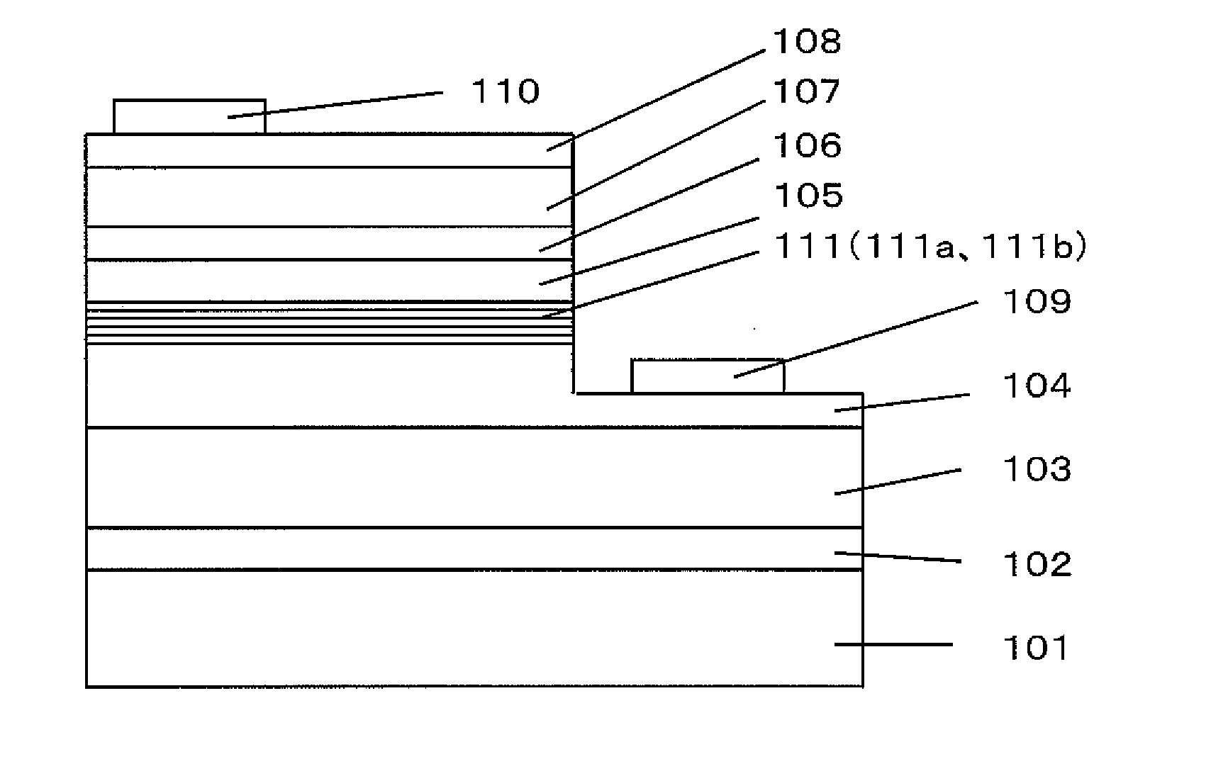
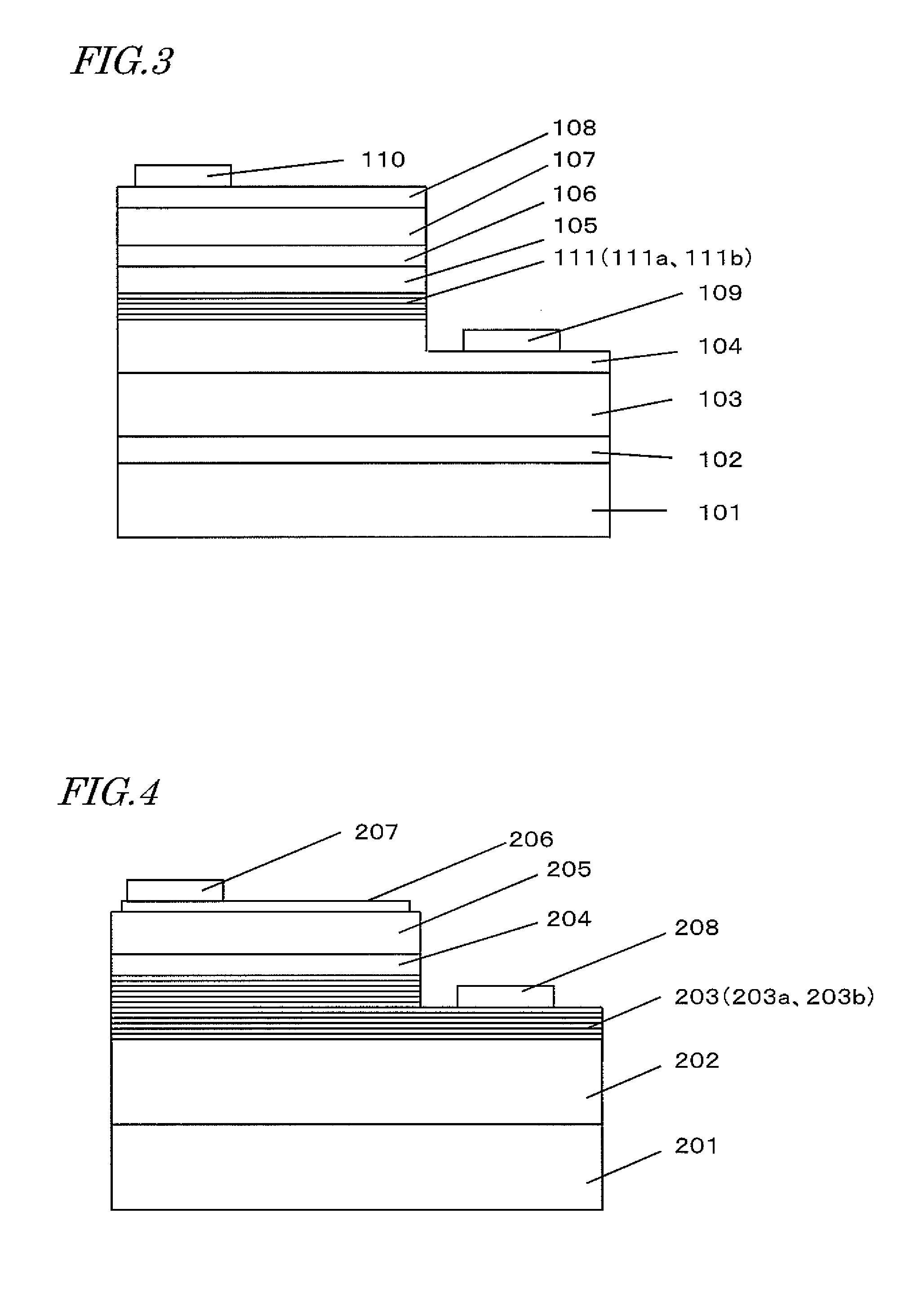
[0067]FIG. 5 is a cross-sectional view showing a structure of a nitride-based semiconductor light-emitting device 31 of the present embodiment. The nitride-based semiconductor light-emitting device 31 has a configuration where a p-electrode 5 and an n-electrode 6 are provided on the same crystal growth surface side (surface electrode type).
[0068]As shown in FIG. 5, the nitride-based semiconductor light-emitting device 31 of the present embodiment includes an n-type GaN substrate (or GaN layer) 1, which has an m-plane principal surface, and a semiconductor multilayer structure 16 provided on the n-type GaN substrate (or GaN layer) 1. The semiconductor multilayer structure 16 includes a current diffusing layer 7, an n-type nitride semiconductor layer 2 provided directly or indirectly on the current diffusing layer 7, an active ...
PUM
 Abstract
Description
Claims
Application Information