

Nano-structured dielectric composite
a dielectric composite and nano-structure technology, applied in the field of nano-structured dielectric composites, can solve the problems of low dielectric constant of the composite, and inability to use high-voltage dielectric materials, etc., to achieve precise multi-layer structure, increase the effect of plasmon resonance effect and high strength
- Summary
- Abstract
- Description
- Claims
- Application Information
AI Technical Summary
Benefits of technology
Problems solved by technology
Method used
Image

Examples
example 1
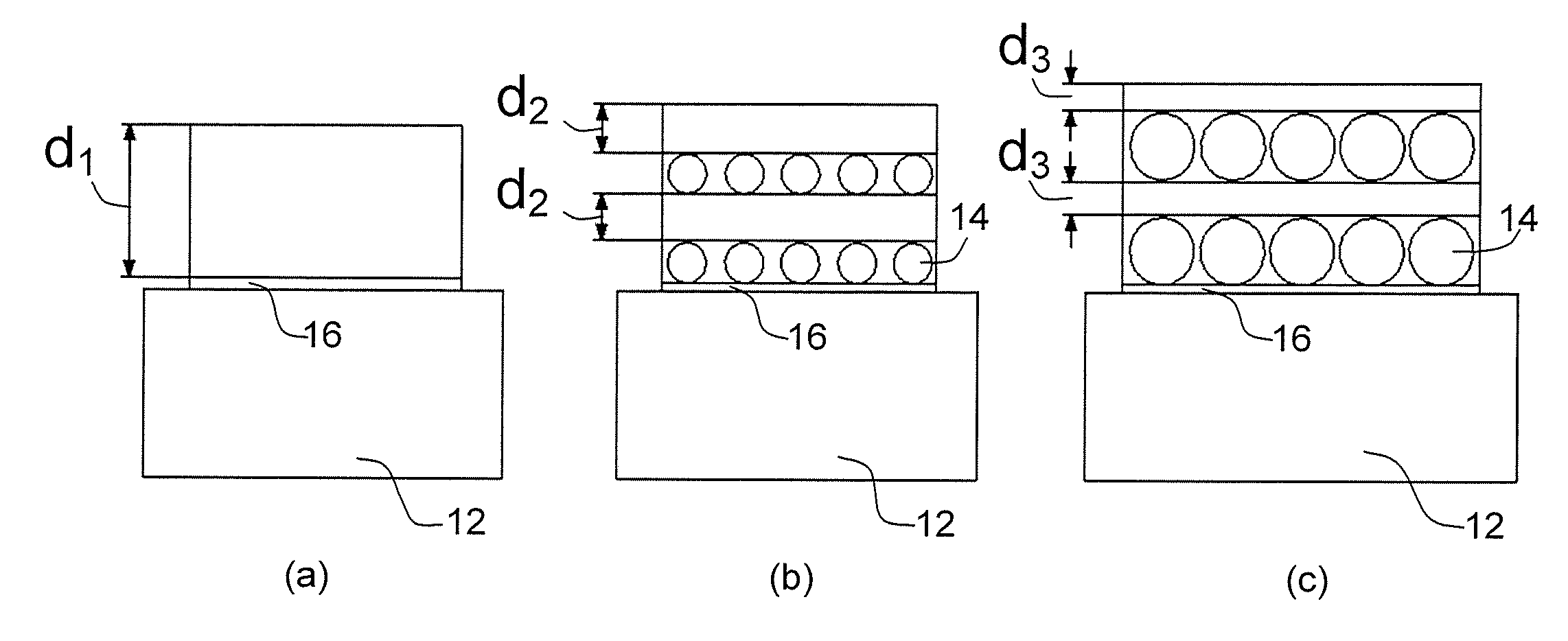
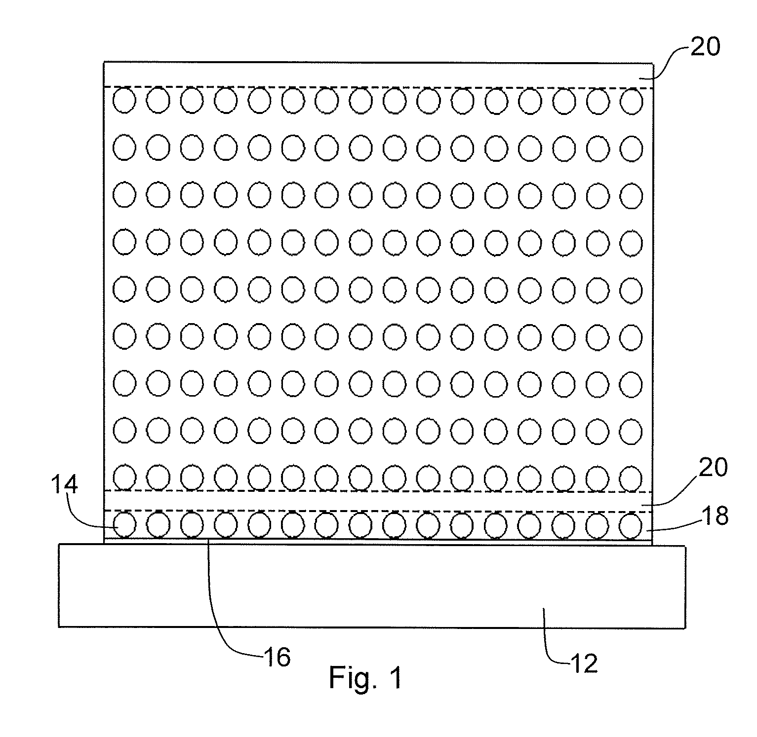
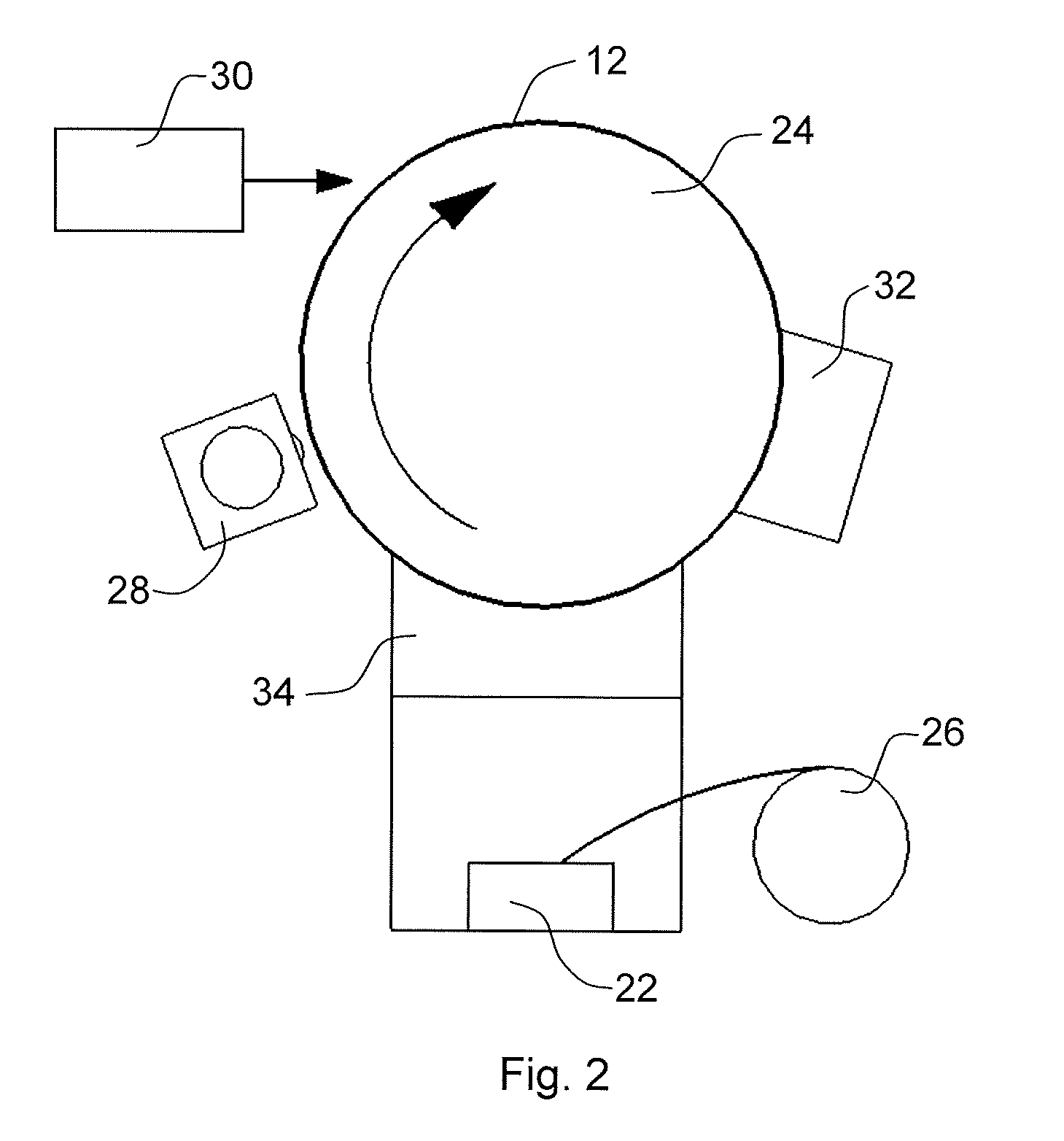
[0032]A metallized polyester film substrate was mounted on a 13 inch wide, 40 inch diameter, rotating drum to allow for electrical measurements. The drum was rotated at a surface speed of 350 ft / min. The monomer vapor was deposited across the entire drum surface and set to produce polymer layers 21-nm thick (in the absence of particles). A silver vapor was produced by feeding two 1-mm diameter wires into two evaporation sources at a fixed rate of 10 ft / min each; the vapor was deposited over only about ⅔ of the drum surface through two different masks positioned adjacent to one another, which allowed the formation of a strip of polymer alone and of two different sizes of silver nanocrystals, one with an average diameter S1 of about 1 nm and the other with an average diameter S2 of 10 nm. A total number of drum revolutions n=120 produced 120 polymer layers; therefore, the portion of multilayer structure without nanoparticles had a total polymer thickness Dp=2520 nm. The portions inclu...
example 2
[0035]The same rotating drum of Example 1 was coated with a release layer and rotated at a surface speed of 500 ft / min. The monomer vapor was deposited across the entire drum surface to produce polymer layers 20-nm thick (in the absence of particles). The width of the drum was partitioned and masked so as to produce four strips of multilayer composite: one with no nanoparticles and three with three different sizes of nanoparticles. Accordingly, the silver vapor, produced as in Example 1, was deposited over only about ¾ of the drum surface to produce a strip with nanoparticles with effective diameters of about 1 nm, 5 nm and 10 nm. A total number of 10,000 drum revolutions were performed to produce a 10,000-layer nanocomposite materials that was separated and lifted off the drum as a self-supported dielectric.
[0036]FIGS. 5(a) and (b) show the spectral response of the 1-nm and 5-nm composites in the Infra Red spectrum, respectively. While the 1-nm particle composite has a response, se...
example 3
[0037]The same drum of Example 1 was rotated at a surface speed of 500 ft / min and the monomer vapor was set to form polymer layers 10-nm thick. A polyester film substrate was mounted on the drum with both metallized and clear areas to allow electrical and optical measurements, respectively. The silver vapor was evaporated at a fixed rate as in Example 1 through three different masks that allowed the formation of three different sizes of silver nanocrystals. Therefore, four different zones were provided on the polyester film for evaluation, as in Example 2. One zone produced polymer only, while the other three zones produced nanocomposites with silver nanoparticles of three different diameters, approximately 1 nm, 5 nm and 10 nm. The total number of deposited layers was 260.
[0038]FIG. 6 shows the UV spectral response of the three nano-structured composites produced in this example. One can clearly see in FIG. 6(a) that the smallest 1-nm diameter nanoparticles exhibit strong and well ...
PUM
| Property | Measurement | Unit |
|---|---|---|
| Thickness | aaaaa | aaaaa |
| Diameter | aaaaa | aaaaa |
| Structure | aaaaa | aaaaa |
Abstract
Description
Claims
Application Information