Power module

a technology of power converters and modules, applied in the field of power modules, can solve the problems of high switch loss, unavoidably needing to use additional materials in the use of semiconductor devices, and the loss of on-state and switch energy consumption of power converters, so as to improve the power density or efficiency of power converters, reduce the cost of thermo-conductive substrates, and improve the effect of power density or efficiency

Active Publication Date: 2012-01-19
DELTA ELECTRONICS INC
View PDF26 Cites 49 Cited by
  • Summary
  • Abstract
  • Description
  • Claims
  • Application Information

AI Technical Summary

Benefits of technology

[0032]As mentioned hereinabove, the power module of one embodiment of the invention is integrated with a plurality of power chips, so the power density or efficiency can be significantly enhanced. In addition, the first power chip of the invention is not disposed on the heat sink through the thermo-conductive insulating layer, and the thermo-conductive insulating layer can be usually implemented by a thermo-conductive substrate. So, the cost of the thermo-conductive substrate can be reduced. In addition, with the package method and structure of the invention capable of enhancing the power density or efficiency of the powe

Problems solved by technology

The energy consumption of the power converter is mainly composed of the on-state loss and the switch loss, especially the switch loss of the active device.
Thus, the high switch loss is induced.
However, the use of the semiconductor device tends to unavoidably need to use the additional materials, such as the package material for protecting the semiconductor, the heat sink for heat dissipating, the fixture for fixing the semiconductor device, and the like, which are not useful to the power converting efficiency.
As the ratio of these materials to the power converter gets greater, the internal space availability of the power converter gets worse.
The package space availability of the semiconductor device becomes a bottleneck.
The different integrated contents cause different consideration points and difficulty levels.
As a result, the package usually has the worse heat dissipating performance.
In addition, because the molding compound has the smaller coefficient of heat conductivity, its transversal thermal diffusing ability is also lower.
Thus, the heat concentration spot (hot spot) tends to occur, thereby decreasing the device reliability and lifetime.
Therefore, the first existing art has the poor heat dissipating ability, and is not suitable for the occasion requiring the high heat dissipating ability.
That is, although the overall heat dissipating performance of this structure is improved, the performance thereof is still poor.
However, all the element devices 32 and 34 need to be mounted on the DBC substrate, so the required area of the DBC carrier is larger, and the price of the DBC substrate is higher, so that the cost is higher.
Because the production technique of the DBC substrate is the high-temperature sintering, the DCB substrate is the product with the high energy consumption, and the use of the large area DBC substrate cannot satisfy the technological progressing trend of the current green environment protection.
However, compared with metal (e.g., the copper with the coefficient equal to about 300 W/m.K), the coefficient difference therebetween is still very large so that the transversal heat diffusion ability is not good enough, and the poor thermal uniformity tends to occur.
However, due to the ap

Method used


Image

  • Power module
  • Power module
  • Power module

Examples


Embodiment Construction

[0040]The present invention will be apparent from the following detailed description, which proceeds with reference to the accompanying drawings, wherein the same references relate to the same elements.

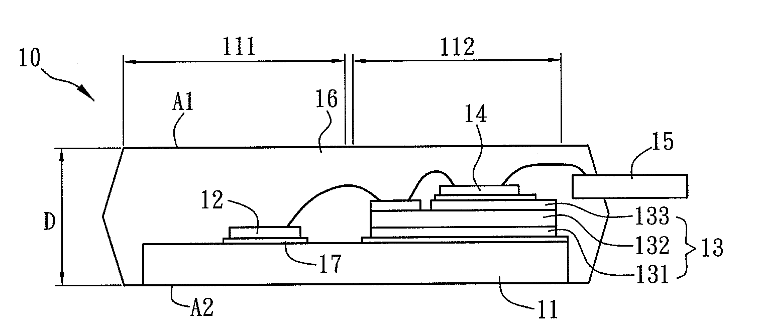
[0041]Referring to FIG. 8, a power module 10 according to a preferred embodiment of the invention may be applied to, for example, a power converter or any other device that requires the power to be converted. The power converter may be an AC / DC or a DC / AC converter or an isolated DC / DC converter. If applied to the power converter, the power module 10 may be applied to a power factor correction (PFC) portion, a DC / DC primary side portion (hereinafter referred to as D2D_Pri) or a DC / DC secondary side portion (hereinafter referred to as D2D_Sec) of the power converter.

[0042]The power module 10 is a package body, which includes a first heat sink 11, a first power chip 12, a thermo-conductive insulating layer 13, a second power chip 14, a lead frame 15 and a molding compound 16. The first ...


PUM

PropertyMeasurementUnit
Thermal conductivityaaaaaaaaaa
Temperatureaaaaaaaaaa

Abstract

A power module includes a first heat sink, first and second power chips, a thermo-conductive insulating layer, a lead frame and a molding compound. The first heat sink has a first area and a second area. The first power chip is disposed in the first area. The thermo-conductive insulating layer is disposed in the second area. The second power chip is disposed on the heat sink through the thermo-conductive insulating layer. The lead frame is electrically connected to at least one of the first and second power chips. The molding compound covers the first and second power chips, the thermo-conductive insulating layer and a portion of the lead frame. The first heat sink is electrically connected to at least one of the first and second power chips. Because the first power chip is not disposed on the first heat sink through the thermo-conductive insulating layer, the cost can be reduced.

Description

CROSS REFERENCE TO RELATED APPLICATIONS[0001]This Non-provisional application claims priority under 35 U.S.C. §119(a) on Patent Application No(s). 201010230160.7 filed in People's Republic of China on Jul. 15, 2010, the entire contents of which are hereby incorporated by reference.BACKGROUND OF THE INVENTION[0002]1. Field of Invention[0003]The invention relates to a power module, and more particularly to a power module applied to a power converter.[0004]2. Related Art[0005]There are more kinds of power converters due to different applications of the power converters. The power converters may be classified into a non-isolated AC / DC power converter, a non-isolated DC / DC power converter, an isolated DC / DC converter, an isolated AC / DC power converter and DC / AC, AC / AC power converters according to the type of the electric energy being converted. The non-isolated AC / DC power converter is, for example, composed of an AC / DC conversion circuit for a power factor correction (hereinafter refer...

Claims


Application Information

Patent Timeline
IPC IPC(8): H05K7/20H05K13/04H05K3/34
CPCH01L23/3107Y10T29/49146H01L23/4952H01L23/49562H01L23/49575H01L24/45H01L24/48H01L25/115H01L2224/32225H01L2224/32245H01L2224/45124H01L2224/45144H01L2224/45147H01L2224/48091H01L2224/48135H01L2224/48137H01L2224/48247H01L2224/4911H01L2224/73265H01L2924/01079H02M7/003H01L23/4334Y10T29/49144H01L2924/01047H01L2924/30107H01L2924/3011H01L2924/13055H01L2924/01013H01L2924/13091H01L2924/01019H01L24/49H01L2924/00014H01L2924/00H01L2224/45015H01L2924/181H01L2224/0603H01L2224/48139H01L2224/4903H01L2924/19107H01L2224/4917H01L2924/00012
Inventor ZENG, JIAN-HONGHONG, SHOU-YUYE, QI-FENGLIN, YI-CHENG
Owner DELTA ELECTRONICS INC
Why Eureka
Try Eureka