

Fabrication of substrates with a useful layer of monocrystalline semiconductor material
a monocrystalline semiconductor and substrate technology, applied in semiconductor/solid-state device manufacturing, basic electric elements, electric instruments, etc., can solve the problems of poor chemical stability under high temperatures, sapphire and silicon carbide are far from being optimal substrate materials, and the lack of large-sized bulk substrates of such materials
- Summary
- Abstract
- Description
- Claims
- Application Information
AI Technical Summary
Benefits of technology
Problems solved by technology
Method used
Image

Examples
example 1
[0086]A 500 nm thick layer of SiO2 is produced on one face of a monocrystalline SiC source substrate by thermal oxidation. Hydrogen ions are then implanted with an energy of 100 keV and using a dose of 8×10¹⁶ ions / cm2 into the source substrate using ion bombardment equipment. A 500 μm thick monocrystalline GaAs substrate intended to form the intermediate support is also prepared, and one face of the substrate is coated with a 500 nm thick SiO2 layer by chemical vapor deposition.
[0087]Surface activation is then carried out, for example by chemical-mechanical polishing, to smooth the surfaces and provide them with a certain hydrophilic nature. The faces of the source substrate and the intermediate support substrate are then brought together and bonded, and a suitable bonding energy is obtained by heat treatment at 350° C. for a period of 2 hours.
[0088]This assembly then undergoes heat treatment at 900° C. for a period of one hour to obtain detachment at the implanted zone. The face of...
example 2
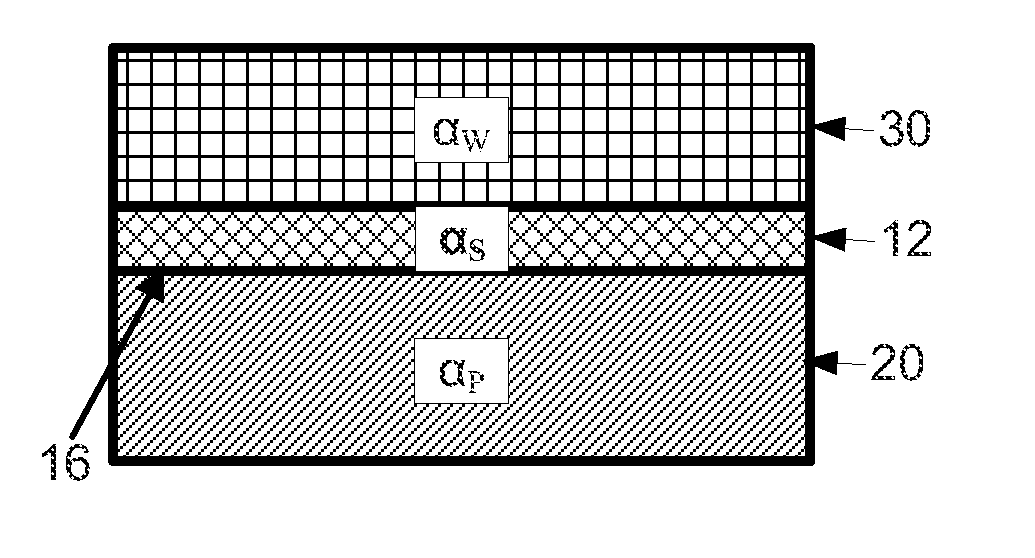
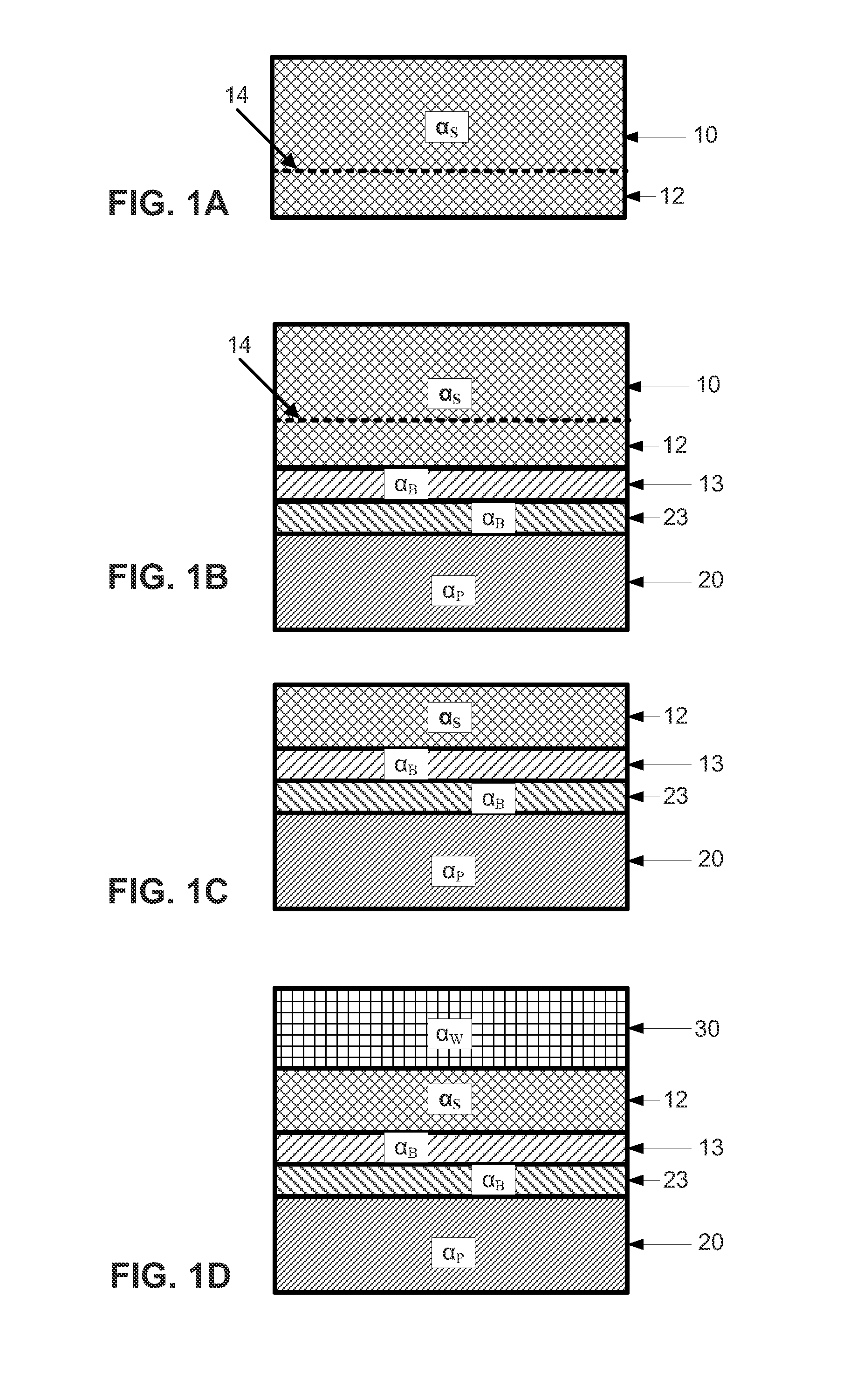
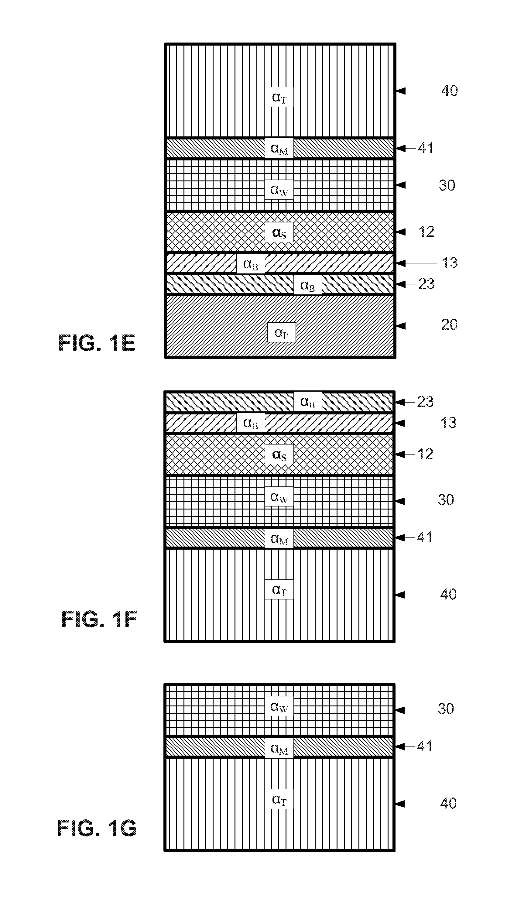
[0092]In accordance with another aspect of the invention, referring to FIGS. 2A to 2E, the technique includes transferring a nucleation layer or seed layer 12 onto a support substrate 20 (illustrated in FIG. 2C), depositing a semiconductor layer or working layer 30 on the seed layer 12 to form a composite substrate (illustrated in FIG. 2D), and then detaching the seed layer 12 and the working layer 30 from the composite substrate (illustrated in FIG. 2E). The seed layer in accordance with this aspect of the invention may comprise material such as sapphire, silicon carbide, zinc oxide, silicon, gallium nitride, neodymium gallate, lithium gallate, or any combination thereof. Also included are other materials commonly known in the art. In an implementation, the seed layer 12 is prepared before receiving the working layer, wherein the preparation may include polishing, annealing, smoothing, oxidation, etching or any combination thereof.
[0093]Preferably the material comprising the seed l...
example 3
[0100]In another embodiment of the method of the invention, a structure is provided comprising a working layer on a seed layer itself on a support with bonding layers and interposed between the seed layer and the support. A thick layer is deposited on the free surface of the working layer and the support is removed, either alone or together with the seed layer. The thick layer then serves in particular to support the working layer, after the seed layer support has been removed.
[0101]In this embodiment, the further layer of the substrate is present upon the working layer on a face opposite that of the seed layer, wherein the further layer preferably is polycrystalline SiC, polycrystalline AlN, polycrystalline GaN, boron nitride, diamond or a metal such a copper.
[0102]Table 2 below summarizes examples of materials that can be used in the context of this second implementation of the method of the invention. These examples are purely illustrative and should not be construed as limiting....
PUM
| Property | Measurement | Unit |
|---|---|---|
| energy | aaaaa | aaaaa |
| temperature | aaaaa | aaaaa |
| temperature | aaaaa | aaaaa |
Abstract
Description
Claims
Application Information