Method and apparatus for processing substrates using a laser

a technology of laser processing and substrate, applied in the field of processing, can solve the problems of shock waves into materials, inability to increase the pulse energy above certain levels, and waste a large portion of semiconductor materials, and achieve the effect of high bending strength of processed components and constant processing quality in tim

Active Publication Date: 2012-03-22
CORELASE
View PDF10 Cites 43 Cited by
  • Summary
  • Abstract
  • Description
  • Claims
  • Application Information

AI Technical Summary

Benefits of technology

[0027]The method according to the invention has found to yield processed substrates having low amount of microcracks within the processed materials and thus high bending strength of processed components (in particul...

Problems solved by technology

This technique has the disadvantage that due to the kerf width, a considerable portion of the semiconductor material is wasted as dust.
In particular, increasing the pulse energy is not possible above certain lev...

Method used


Image

  • Method and apparatus for processing substrates using a laser
  • Method and apparatus for processing substrates using a laser
  • Method and apparatus for processing substrates using a laser

Examples


Embodiment Construction

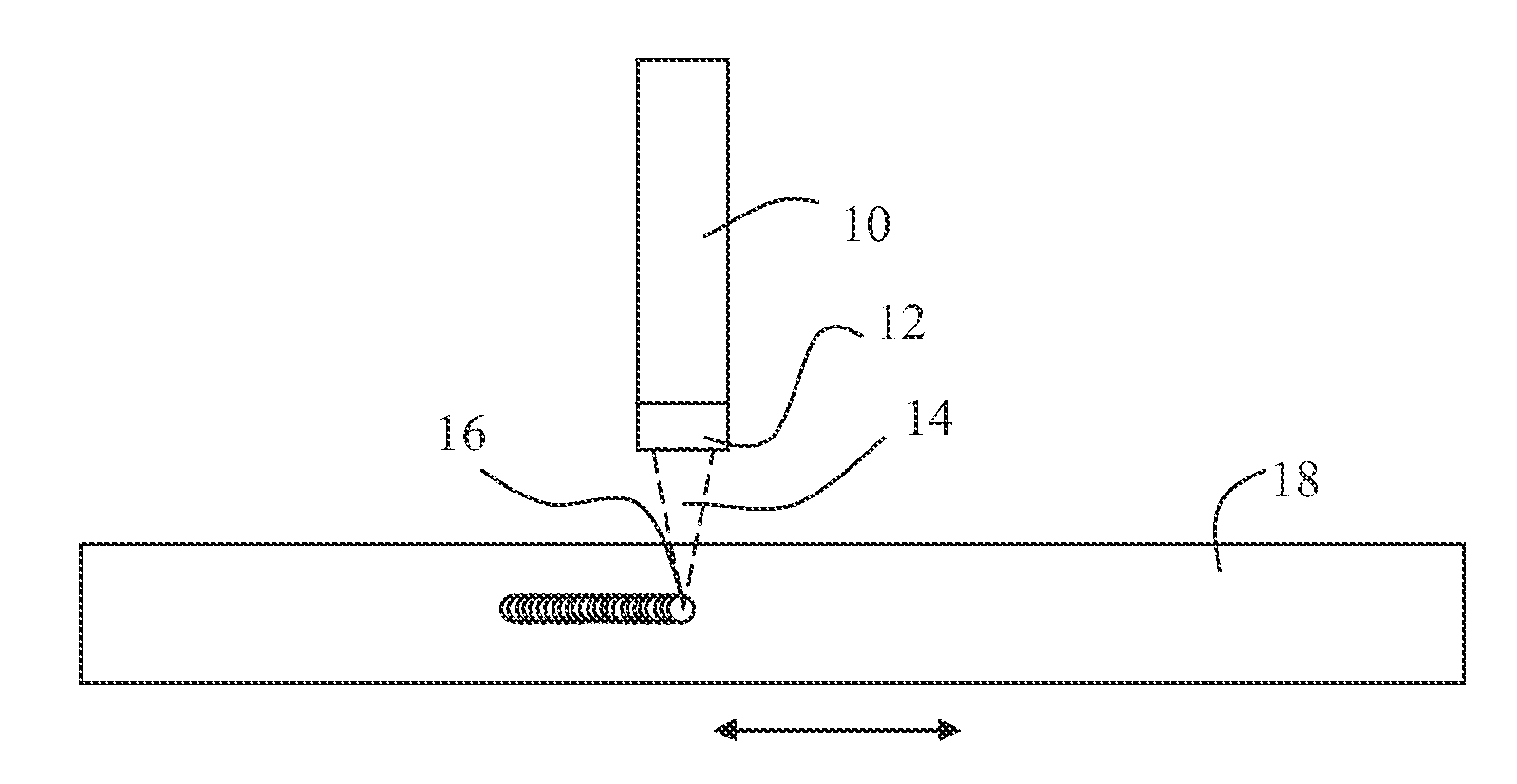
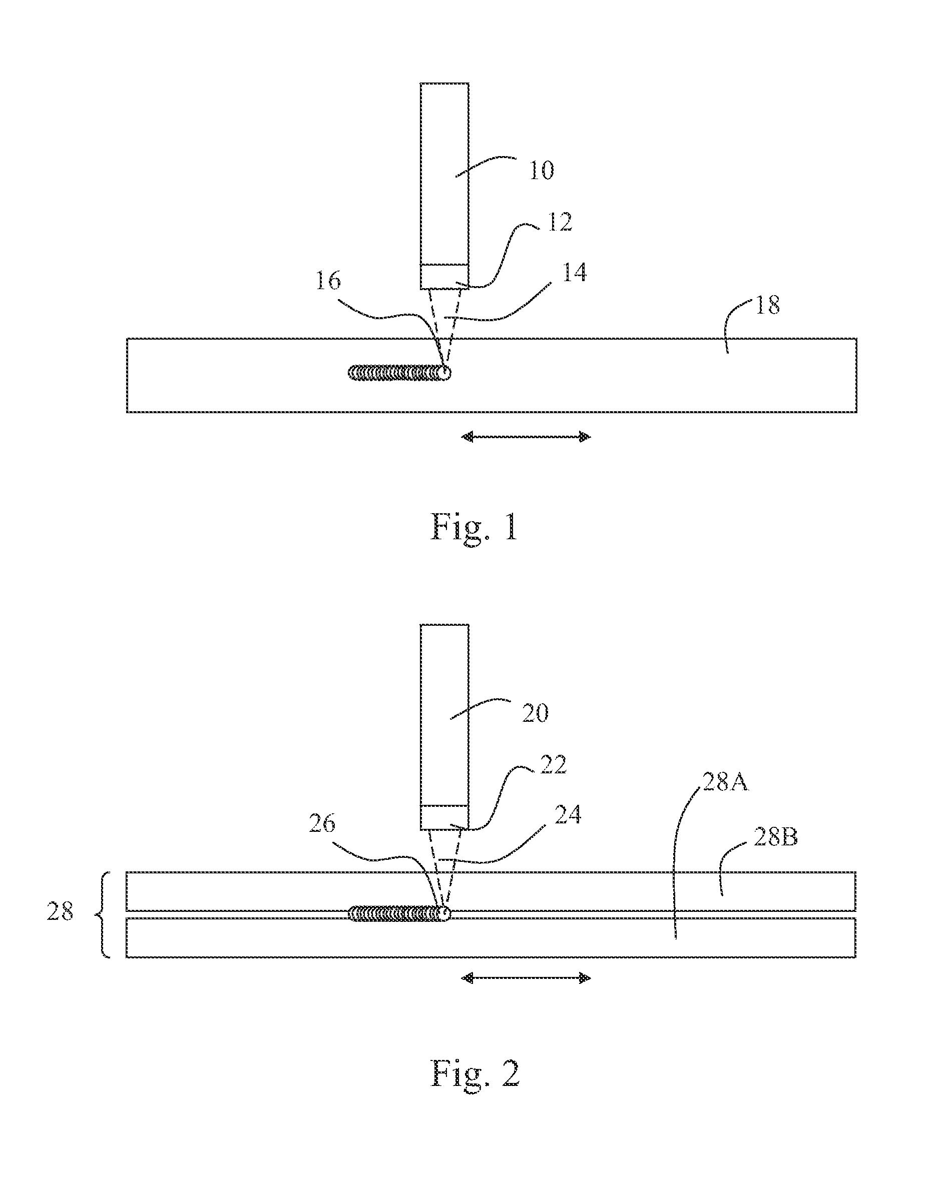
[0040]The invention comprises producing to a substrate structurally modified lines using pulsed laser having a pulse duration of at least 20 ps and a pulsing frequency which is matched with processing velocity such that a plurality of the pulses synergistically increase absorption within the substrate. In particular, if the distance between successive pulses is less than ⅕ of the diameter of the focal spot of the laser beam, many enough pulses arrive to a very local region of the substrate such that the synergetic effect is ensured. In typical applications, the focal spot diameter is in the range of 1-10 μm, resulting in a typical maximum distance between pulses the range of 200 nm-2 μm.

[0041]According to one embodiment, the pulse duration used is at least 25 ps.

[0042]According to one embodiment, the pulsing frequency is increased or the moving velocity is decreased such that the distance between successive structurally modified spots is less than 1 / 10, preferably less than 1 / 20 of ...


PUM

PropertyMeasurementUnit
Timeaaaaaaaaaa
Thicknessaaaaaaaaaa
Lengthaaaaaaaaaa

Abstract

The invention relates to a method and apparatus for processing substrates, such as glass and semiconductor wafers. The method comprises directing to the substrate from a laser source a plurality of sequential focused laser pulses having a predetermined duration, pulsing frequency and focal spot diameter, the pulses being capable of locally melting the substrate, and moving the laser source and the substrate with respect to each other at a predetermined moving velocity so that a structurally modified zone is formed to the substrate. According to the invention, the pulse duration is in the range of 20-100 ps, pulsing frequency at least 1 MHz and moving velocity adjusted such that the distance between successive pulses is less than ⅕ of the diameter of the focal spot. The invention can be utilized, for example, for efficient dicing, scribing and welding of materials which are normally transparent.

Description

FIELD OF THE INVENTION[0001]The invention relates to processing, such as cutting, dicing and welding of materials and substrates using laser. In particular, the invention relates to processing of glass and semiconductor substrates, e.g. sapphire, quartz and silicon substrates and the like. The invention also concerns a novel laser apparatus and novel uses of laser sources.BACKGROUND OF THE INVENTION[0002]Conventionally semiconductor wafers are diced using mechanical sawing after manufacturing of semiconductor structures on the wafer. This technique has the disadvantage that due to the kerf width, a considerable portion of the semiconductor material is wasted as dust. According to some estimates, this means at least hundreds, if not thousands of tons of silicon waste annually in the global scale.[0003]Also laser light can be used for dicing of semiconductor wafers after manufacturing of semiconductor structures on the wafer. Generally, in such methods, a cutting line is produced by l...

Claims


Application Information

Patent Timeline
IPC IPC(8): B23K26/00
CPCB23K26/0635B23K26/246B23K26/3266C03C23/0025B28D5/0011C03B33/0222C03B33/082B23K2201/40B23K26/0624B23K26/244B23K26/32B23K2101/40B23K2103/50Y02P40/57
Inventor KANGASTUPA, JARNOAMBERLA, TIINA
Owner CORELASE
Why Eureka
Try Eureka