Target of Sintered Compact, and Method of Producing the Sintered Compact

Active Publication Date: 2012-04-26
JX NIPPON MINING& METALS CORP
View PDF2 Cites 7 Cited by
  • Summary
  • Abstract
  • Description
  • Claims
  • Application Information

AI Technical Summary

Benefits of technology

[0025]Conventionally, when preparing a target of sintered compact by using a chalcogenide element (A) and a Vb-group element (B), or using the elements (A) and (B) and additionally a IVb-group element or a IIIb-group element (C) as the raw powder, for instance, with a Ge22.2-Sb22.2-Te55.6 at % sintered compact as the representative example thereof, it was possible to only obtain a sintered compact with electric resistivity exceeding 0.30 mΩ·cm and with thermal conductivity of less than 2.5 W/mK, and DC sputtering could not be adopted for sputtering deposition. This has lead to the generation of arcing and the generation of particles.
[0026]Moreover, since the thermal conductivity is low as described above, heat tends to accumulate within the target. Thus, components with high vapor pressure become volatilized, and it was not possible to avoid the variation in the deposited film composition associated with the progress of sputtering and the generation of particles caused by the volatile components.
[0027]Contrary to the results shown in the prior arts, the composition of raw material for producing the sintered compact, and the processing and s

Problems solved by technology

Nevertheless, these materials generally have low thermal conductivity and low electric conductivity.
A target produced from this kind of sintered compact with low thermal conductivity and low electric conductivity often entails such problems particularly caused by low thermal conductivity where components with high vapor pressure become volatilized and particles are generated easily due to the heat generated by the sputtering being accumulated within the target.
In addition, there is a problem such as charge-up with DC sputtering, and it is necessary to take measures such as using the pulsed DC sputtering technique to perform the deposition.
Still, it is impossible to completely eliminate drawbacks such as arcing caused by the charge-up, and there is a problem in that the deposition efficiency is low.
However, since oxygen is consumed during the deposition process, there is a problem in that the amount of oxygen will fluctuate during the deposition unless the amount of oxygen gas in the sputtering atmosphere is strictly controlled.
Thus, this technology is heading in a direction that is opposite to improving the electric conduction and thermal conduction, and cannot be used as a technical guideline for increasing the thermal conductivity and electric conductivity of the target in order to perform stable DC sputtering.[Patent Document 1] Japanese Laid-Open Patent Publication No. 2004-311729[Patent Document 2] Japanese Laid-Open Patent Publication No.

Method used


Image

  • Target of Sintered Compact, and Method of Producing the Sintered Compact
  • Target of Sintered Compact, and Method of Producing the Sintered Compact

Examples


example 1

[0064]The raw powders of Te, Sb and Ge respectively having a purity of 99.999% (5N) excluding gas components were mixed and melted to obtain a composition of Ge22.2Sb22.2Te55.6 (at %), and slowly cooled in a furnace to prepare a cast ingot.

[0065]The raw materials of the respective elements were subject to acid cleaning and deionized water cleaning prior to the melting process in order to sufficiently eliminate impurities remaining particularly on the surface.

[0066]Consequently, a high-purity Ge22.2Sb22.2Te55.6 ingot maintaining a purity of 99.999% (5N) was obtained. Subsequently, the high-purity Ge22.2Sb22.2Te55.6 ingot was pulverized with a ball mill to prepare raw powder having an average grain size of approximately 30 μm, and a maximum grain size of approximately 90 μm (the values were round to the 10).

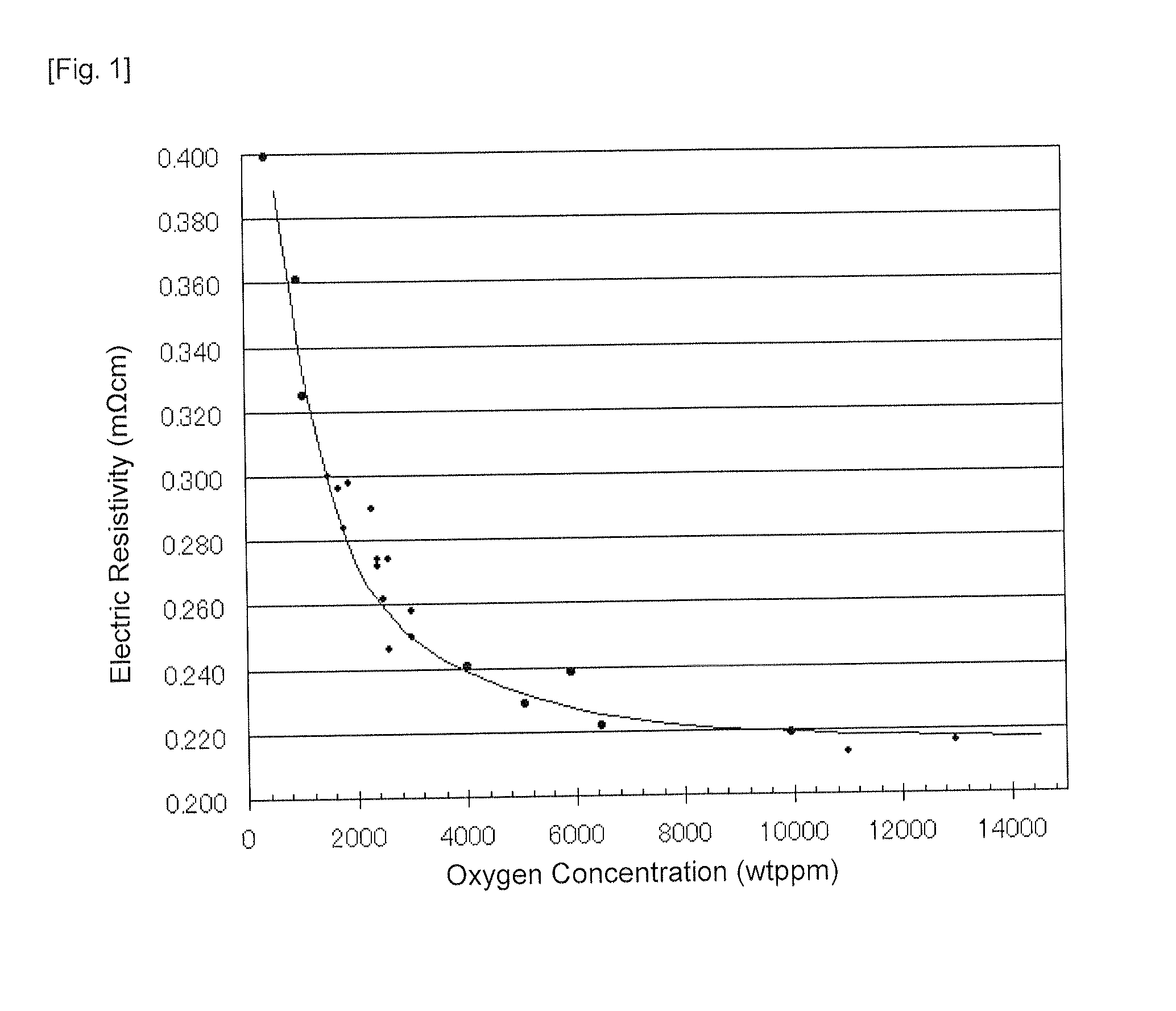
[0067]This raw powder was oxidized by being subject to heat treatment for 6 hours at 350° C. in the atmosphere (oxygen concentration: 20.90%). The oxygen content was 5000 wtppm.

[00...

example 2

[0072]The same raw powder as Example 1 was used up to the pulverization process, and this raw powder was oxidized by being subject to heat treatment for 12 hours at 350° C. in the atmosphere (oxygen concentration: 20.90%). The oxygen content of the raw powder was 7500 wtppm. The subsequent sintering conditions and final HIP treatment conditions were the same as Example 1 for manufacturing a sputtering target.

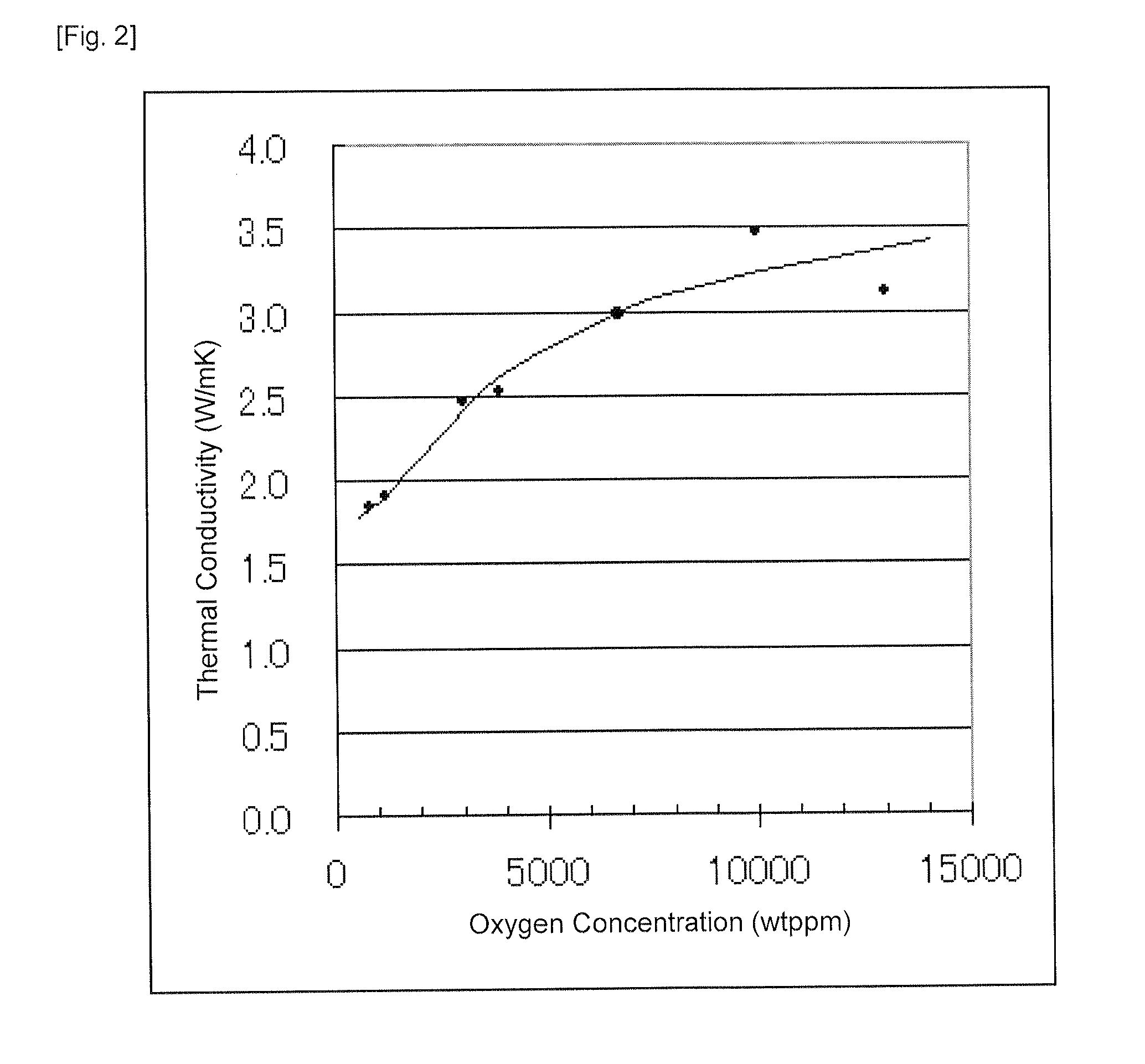
[0073]The thermal conductivity of the target material manufactured as described above was 3.2 W / mK, and the electric resistivity was 0.24 mΩ·cm. This target material was bonded with a copper alloy backing plate to obtain a sputtering target.

[0074]DC (direct current) magnetron sputtering was performed using this sputtering target. The DC (direct current) magnetron sputtering could be performed even easier than Example 1, and the sputtering rate increased.

[0075]The arcing generation rate was less than once per minute and the particle generation rate was 20 particles or less. The p...

example 3

[0076]The same raw powder as Example 1 was used up to the pulverization process, and this raw powder was subject to heat treatment for 24 hours at 350° C. in a high oxygen atmosphere (oxygen concentration in the atmosphere was increased so as to achieve an oxygen concentration of 50%). The oxygen content of the raw powder was 10000 wtppm.

[0077]The subsequent sintering conditions and final HIP treatment conditions were the same as Example 1 for manufacturing a sputtering target. The thermal conductivity of the target material manufactured as described above was 3.5 W / mK, and the electric resistivity was 0.22 mΩ·cm. This target material was bonded with a copper alloy backing plate to obtain a sputtering target.

[0078]DC (direct current) magnetron sputtering was performed using this sputtering target. The DC (direct current) magnetron sputtering could be performed even easier than Example 1 and Example 2, and the sputtering rate was extremely high.

[0079]The arcing generation rate was le...


PUM

PropertyMeasurementUnit
Fractionaaaaaaaaaa
Fractionaaaaaaaaaa
Fractionaaaaaaaaaa

Abstract

Provided is a target of sintered compact essentially consisting of an element of (A), an element of (B) and an element of (C) below, wherein the thermal conductivity is 2.5 W / mK or more and the oxygen concentration is 5000 ppm or more:(A) one or more chalcogenide elements selected from S, Se, and Te;(B) one or more Vb-group elements selected from Bi, Sb, As, P, and N; and(C) one or more IVb-group elements or IIIb-group elements selected from Ge, Si, C, Ga, and In. Also provided is a technology enabling stable DC sputtering, and stable and high-speed sputtering by applying high electric power, by improving heat accumulation and diffusion of volatile components due to the sputtering target having high thermal conductivity and low electric resistivity.

Description

TECHNICAL FIELD[0001]The present invention relates to a target of sintered compact containing a Vb-group element (A) and a chalcogenide element (B), or containing the elements (A) and (B) and additionally a IVb-group element and / or a IIIb-group element (C), in which the electric resistivity of the sintered compact is reduced, as well as to a method of producing such a target. Note that this material containing a Vb-group element (A) and a chalcogenide element (B), or containing the elements (A) and (B) and additionally a IVb-group element and / or a IIIb-group element (C), in which the electric resistivity of the sintered compact is reduced, is hereinafter abbreviated as the “Ge—Sb—Te-based material”.BACKGROUND ART[0002]In recent years, a thin film formed from the Ge—Sb—Te-based material is being used as a material for phase-change recording; that is, as a medium for recording information by using phase transformation.[0003]As a method of forming this thin film of the Ge—Sb—Te-based a...

Claims


Application Information

Patent Timeline
IPC IPC(8): C23C14/34
CPCC23C14/0623H01C17/12H01C7/006C23C14/3414C23C14/35H01J37/3414H01J37/3426
Inventor TAKAHASHI, HIDEYUKI
Owner JX NIPPON MINING& METALS CORP
Why Eureka
Try Eureka