
Photoelectric conversion device and solid-state imaging device

Active Publication Date: 2012-04-26
FUJIFILM CORP
View PDF2 Cites 17 Cited by
  • Summary
  • Abstract
  • Description
  • Claims
  • Application Information

AI Technical Summary

Benefits of technology

[0010]The present invention has been made in an effort to provide a photoelectric conversion device and a solid-state imaging device that can obtain sufficient sensitivity and heat resistance, and exhibit a high speed response property.
[0011]In the organic photoelectric conversion device, in order to implement a high photoelectric conversion efficiency, a low dark current property, and a high speed response property, it is required that the used organic photoelectric conversion film (photoelectric conversion layer) satisfies the following requirements. 1. With respect to the high efficiency and the high speed response, it is required that a signal charge can be rapidly transferred to both electrodes without loss after an exciton is dissociated. It is required that the number of sites trapping carriers is small, mobility is high, and electric charge transportability is high. 2. With respect to the high photoelectric conversion efficiency, it is preferable that stabilization energy of the exciton is low, and the exciton is rapidly dissociated (high exciton dissociation efficiency) by an electric field applied from the outside, or an electric field generated in the inside by a pn-junction. 3. In order to decrease the carriers generated in the inside under a dark state as much as possible, it is preferable to select a film structure and a material having a small amount of impurities which are one of the factors of an intermediate level of the inside. 4. In the case where a plurality of layers is laminated, it is required that energy levels of adjacent layers are matched, and the electric charge transporting is obstructed if an energy barrier is formed.
[0013]In the case where an organic photoelectric conversion film is formed, a deposition method is preferable in that thermal decomposition is suppressed during the deposition as a decomposition temperature is increased compared to a deposition feasible temperature. An application coating method is preferable in that a film is formed without subjecting to a limitation by the decomposition as described above, and a low cost can be realized. However, since uniform film formation is facilitated and a possibility of introducing impurities is reduced, formation of the film by the deposition method is preferable.
[0014]The present inventor has extensively examined and found out that the following selection and combination of materials as a means for capable of satisfying the above requirements and realizing high photoelectric conversion efficiency, low dark current property, high speed response property and heat resistance.

Problems solved by technology

In the case where a plurality of layers is laminated, it is required that energy levels of adjacent layers are matched, and the electric charge transporting is obstructed if an energy barrier is formed.

Method used


Image

  • Photoelectric conversion device and solid-state imaging device
  • Photoelectric conversion device and solid-state imaging device
  • Photoelectric conversion device and solid-state imaging device

Examples


example

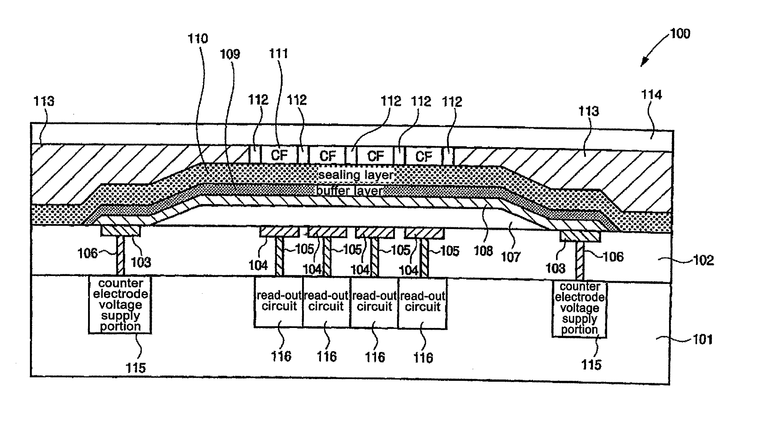
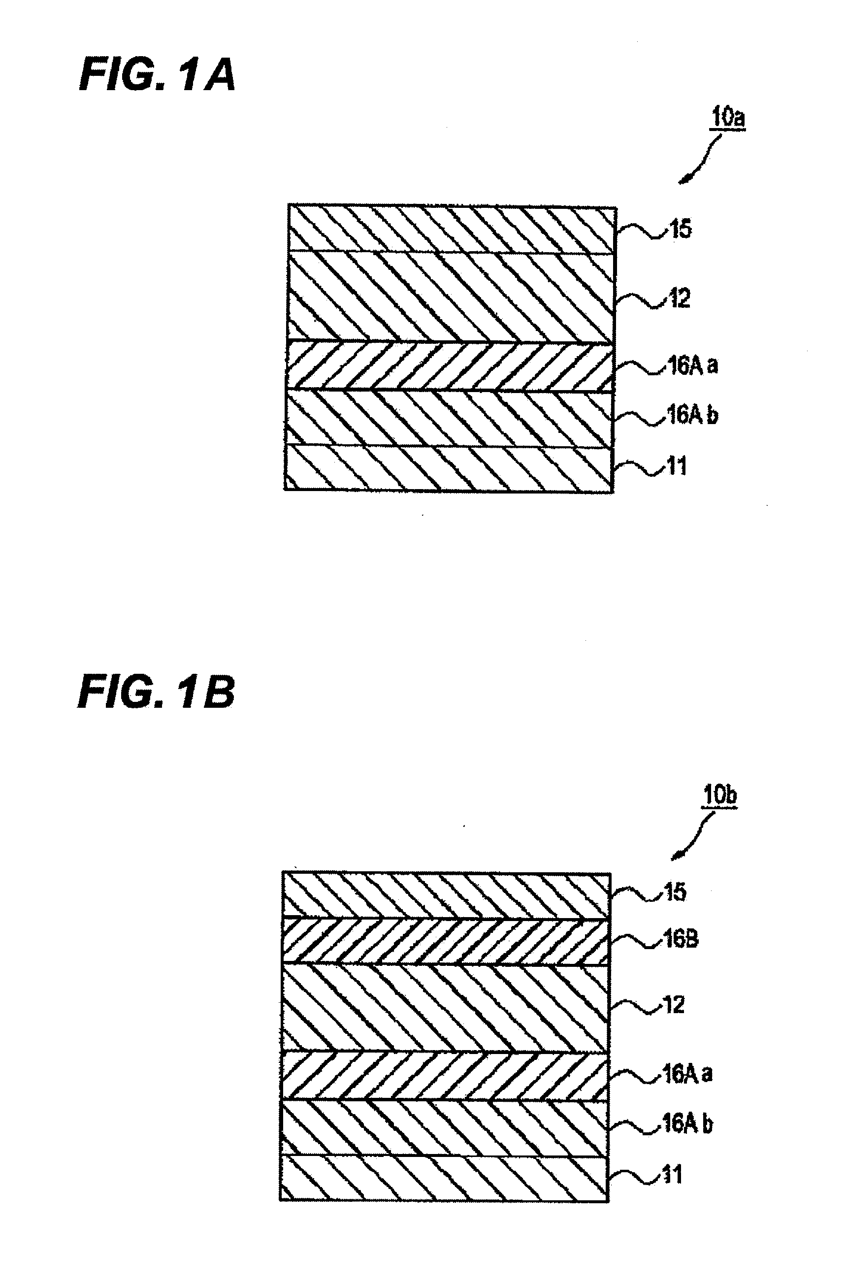
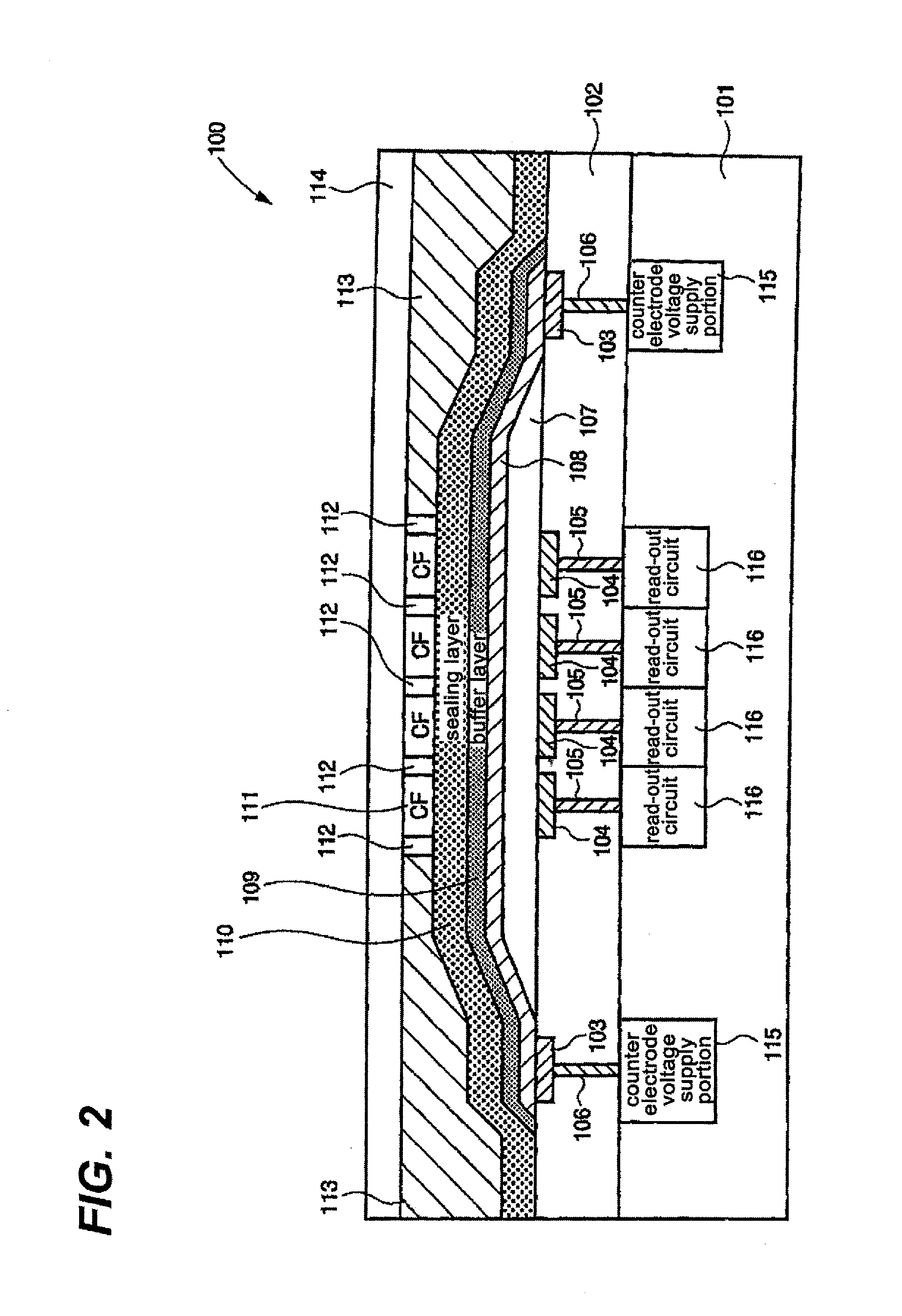
[0181]There is the photoelectric conversion device constituted by the lower electrode / the electron blocking layer 1 / the electron blocking layer 2 (mixed layer) / the photoelectric conversion layer / the upper electrode / the sealing layer, which are sequentially formed. The electron blocking layer 1 is the electron blocking layer in which the content of a fullerene or a fullerene derivative is the volume ratio of 10% or less. The layer in which the electron blocking layer 1 and the mixed layer are mixed is the electron blocking layer. The electron blocking layer 1, the mixed layer, the photoelectric conversion layer, and the upper electrode were sequentially formed on the lower electrode. The lower electrode is TiN. The electron blocking layer 1 was formed in the film thickness of 60 nm by using the organic compound represented by compound 1 by the vacuum deposition method. In the mixed layer, the mixed layer of the organic compound represented by the compound 1 and C60 (compound 1:C60=1:...

examples 2 to 4 , 6 to 8 , 10 to 12 , 14 to 16 , 18 to 20 , 22 to 31

Examples 2 to 4, 6 to 8, 10 to 12, 14 to 16, 18 to 20, 22 to 31

[0182]As shown in Tables 3 to 16, the devices of Examples 2 to 4, 6 to 8, 10 to 12, 14 to 16, 18 to 20, and 22 to 31 were manufactured in the same manner as Example 1 by changing the materials of the electron blocking layer 1, the electron blocking layer 2 (mixed layer), and the photoelectric conversion layer (bulk hetero layer), and the mixing ratio and the film thickness of the materials.

example 5

[0183]There is the photoelectric conversion device constituted by the lower electrode / electron blocking layer 2 (mixed layer) / the photoelectric conversion layer / the upper electrode / the sealing layer, which are sequentially formed. The electron blocking layer 2 (mixed layer), the photoelectric conversion layer, and the upper electrode are formed in this order. The lower electrode is TiN. In the mixed layer, the mixed layer of the organic compound represented by the compound 1 and C60 (compound 1:C60=1:1 (volume ratio)) was formed in the film thickness of 100 nm under the vacuum by the co-deposition. In the photoelectric conversion layer, the mixed layer of the organic compound represented by the compound 2 and C60 (compound 2:C60=1:2 (volume ratio)) was formed in the film thickness of 400 nm under the vacuum by the co-deposition. The upper electrode was formed of ITO in the film thickness of 10 nm by the high frequency magnetron sputter. The sealing layer was formed of the laminate f...


PUM


Abstract

A photoelectric conversion device having: a pair of electrodes; a photoelectric conversion layer sandwiched between the pair of electrodes; and at least one electron blocking layer provided between one electrode of the pair of electrodes and the photoelectric conversion layer, wherein the photoelectric conversion layer contains at least one organic material, and the at least one electron blocking layer has a mixed layer containing fullerene or fullerene derivatives.

Description

CROSS-REFERENCE TO RELATED APPLICATION(S)[0001]The present application claims priority from Japanese Patent Application No. 2010-240185 filed on Oct. 26, 2010, the entire content of which is incorporated herein by reference.BACKGROUND[0002]1. Field[0003]The present invention relates to a solid-state imaging device and a solid-state imaging device useful in a photosensor, a photoelectric conversion device.[0004]2. Description of Related Art[0005]A conventional photosensor in general is a device fabricated by forming a photodiode (PD) in a semiconductor substrate such as silicon (Si), and as for the solid-state imaging device, a flat solid-state imaging device is widely used where PDs are two-dimensionally arranged in a semiconductor substrate and a signal according to a signal charge generated by photoelectric conversion in each PD is read out through a CCD or CMOS circuit.[0006]Development of a photoelectric conversion device using an organic compound is on the way. An organic photo...

Claims


Application Information

Patent Timeline
IPC IPC(8): H01L27/146H01L31/0232H01L31/02B82Y99/00
CPCB82Y10/00H01L51/0046H01L51/0058Y02E10/549H01L51/0072H01L51/4273H01L51/006Y02P70/50H10K85/211H10K85/626H10K85/633H10K85/6572H10K39/00H01L27/146H10K30/353
Inventor SUZUKI, HIDEYUKI
Owner FUJIFILM CORP
Learn More