Method of Fabricating Optical Devices Using Laser Treatment of Contact Regions of Gallium and Nitrogen Containing Material

a technology of nitrogen-containing material and laser treatment, which is applied in the direction of lasers, semiconductor lasers, solid-state devices, etc., can solve the problems of inability to modulate lasers at high speed, inconvenient operation, and inability to meet the needs of lasers, and achieve the effect of improving device performan

Active Publication Date: 2012-05-03
KYOCERA SLD LASER INC
View PDF7 Cites 160 Cited by
  • Summary
  • Abstract
  • Description
  • Claims
  • Application Information

AI Technical Summary

Benefits of technology

[0008]According to the invention, techniques related generally to optical devices are provided. In particular, the invention provides a method and device for emitting electromagnetic radiation using nonpolar gallium containing substrates such as GaN, MN, InN, InGaN, AlGaN, and AlInGaN, and others. More particularly, the present method and device uses a laser scribing process to ablate a portion of a cont

Problems solved by technology

The Ar-ion laser had the benefit of producing highly directional and focusable light with a narrow spectral output, but the efficiency, size, weight, and cost of the lasers were undesirable.
As laser technology evolved, more efficient lamp pumped solid state laser designs were developed for the red and infrared wavelengths, but these technologies remained a challenge for blue and green and blue lasers.
The resulting green and blue lasers were called “lamped pumped solid state lasers with second harmonic generation” (LPSS with SHG) and were more efficient than Ar-ion gas lasers, but were still too inefficient, large, expensive, fragile for broad deployment outside of specialty scientific and medical applications.
Additionally, the gain crystal used in the solid

Method used


Image

  • Method of Fabricating Optical Devices Using Laser Treatment of Contact Regions of Gallium and Nitrogen Containing Material
  • Method of Fabricating Optical Devices Using Laser Treatment of Contact Regions of Gallium and Nitrogen Containing Material
  • Method of Fabricating Optical Devices Using Laser Treatment of Contact Regions of Gallium and Nitrogen Containing Material

Examples


example

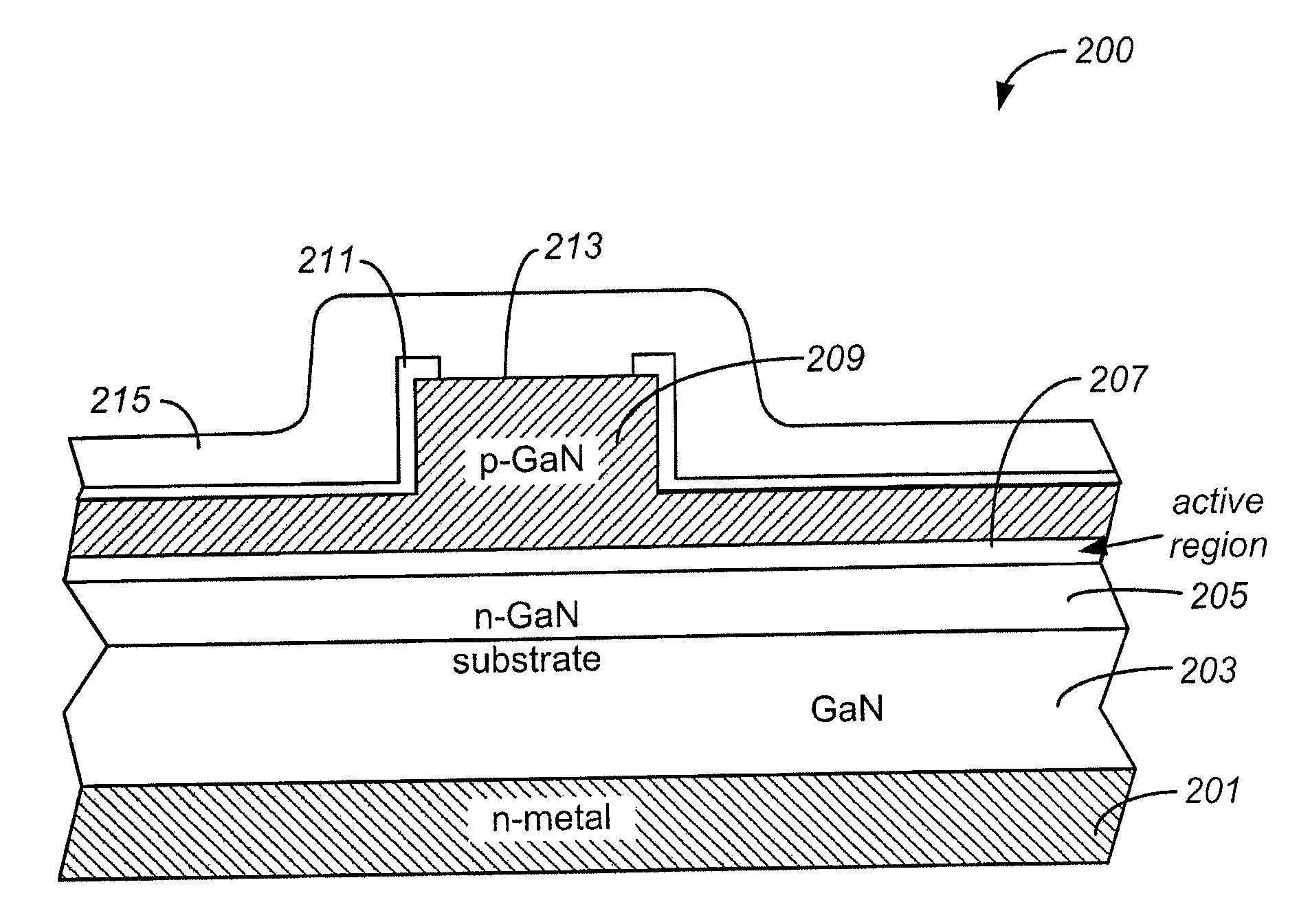
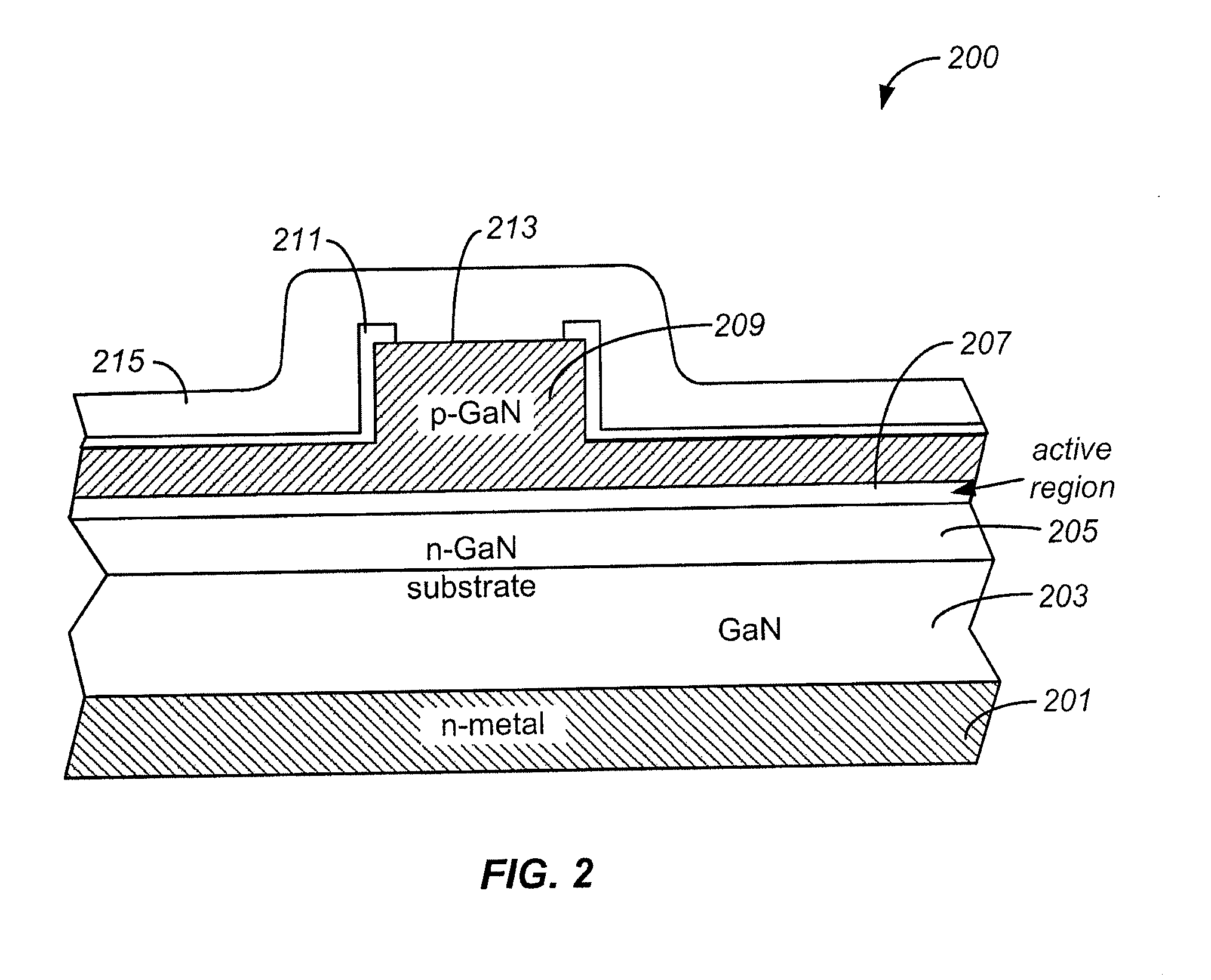
[0128]FIGS. 19, 20(A), and 20(B) are diagram illustrating experimental results of a laser scribing process for contact formation according to the invention. FIG. 19 shows an IV curve from a set of Transmission Line Models (TLM's) that were fabricated on top of 4 different GaN backside surfaces: lapped, lapped and laser scribed, lapped and polished, and lapped, polished and laser scribed. As used herein, TLM stands for Transmission Line Model, which is a measure technique for resistance of contacts along with the sheet resistance of the one or more materials having the deposited metallization contacts. Typically the measurements are performed by varying the distances between the two metal contacts and plotting resistance versus distance of the contacts. From the line that is formed on the plot, the contact resistance and the sheet resistance are deduced. As shown are current versus voltage curves in the plots. The curves are for the different n-contact schemes on the same or similar ...


PUM


Abstract

A method for forming optical devices includes providing a gallium nitride substrate having a crystalline surface region and a backside region. The backside is subjected to a laser scribing process to form scribe regions. Metal contacts overly the scribe regions.

Description

REFERENCE TO RELATED APPLICATION[0001]This application is a continuation-in-part and claims priority from U.S. patent application Ser. No. 12 / 942,817, filed Nov. 9, 2010 which is entitled: “Method of Fabricating Optical Devices Using Laser Treatment.” That application is incorporated by reference herein.BACKGROUND OF THE INVENTION[0002]The invention is directed to optical devices and related methods. In particular, the invention provides a method and device for emitting electromagnetic radiation using nonpolar gallium containing substrates such as GaN, MN, InN, InGaN, AlGaN, and AlInGaN, and others. More particularly, the present method and device uses a laser scribing process to ablate a portion of a contact region for improved device performance. Merely by way of example, the invention can be applied to optical devices, lasers, light emitting diodes, solar cells, photoelectrochemical water splitting and hydrogen generation, photodetectors, integrated circuits, and transistors, amo...

Claims


Application Information

Patent Timeline
IPC IPC(8): H01L33/06H01L33/32
CPCB82Y20/00H01L33/0095H01L33/20H01S5/0202H01S5/0217H01S5/028H01S5/0425H01L2924/0002H01S5/2201H01S5/3202H01S5/34333H01S2304/04H01L2924/00H01S5/04254H01S5/32025
Inventor FELKER, ANDREWVICKERS, NICHOLAS A.ALDAZ, RAFAELPRESS, DAVIDPFISTER, NICHOLAS J.RARING, JAMES W.SCHMIDT, MATHEW C.THOMSON, KENNETH JOHN
Owner KYOCERA SLD LASER INC
Why Eureka
Try Eureka