
Organic electroluminescent display device
a display device and electroluminescent technology, applied in the direction of electroluminescent light sources, thermoelectric devices, electric lighting sources, etc., can solve the problems of insufficient inability to provide inability to achieve sufficient out-coupling efficiency of light, etc., to achieve high electron injection properties, low absorption, and high reflectance
- Summary
- Abstract
- Description
- Claims
- Application Information
AI Technical Summary
Benefits of technology
Problems solved by technology
Method used
Image

Examples
first embodiment
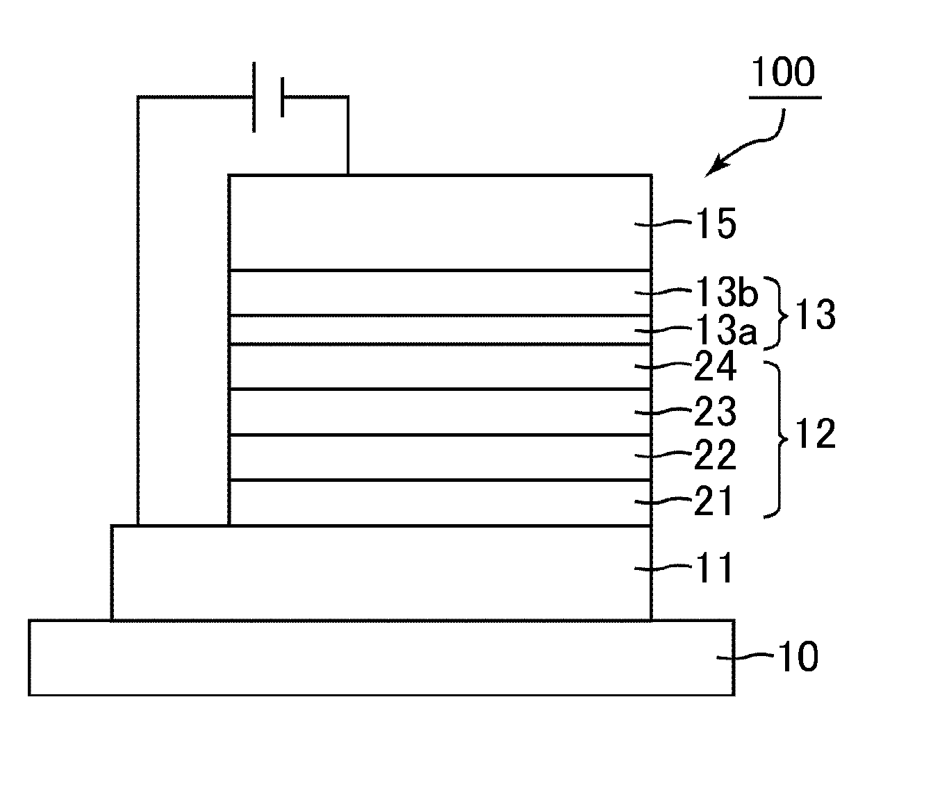
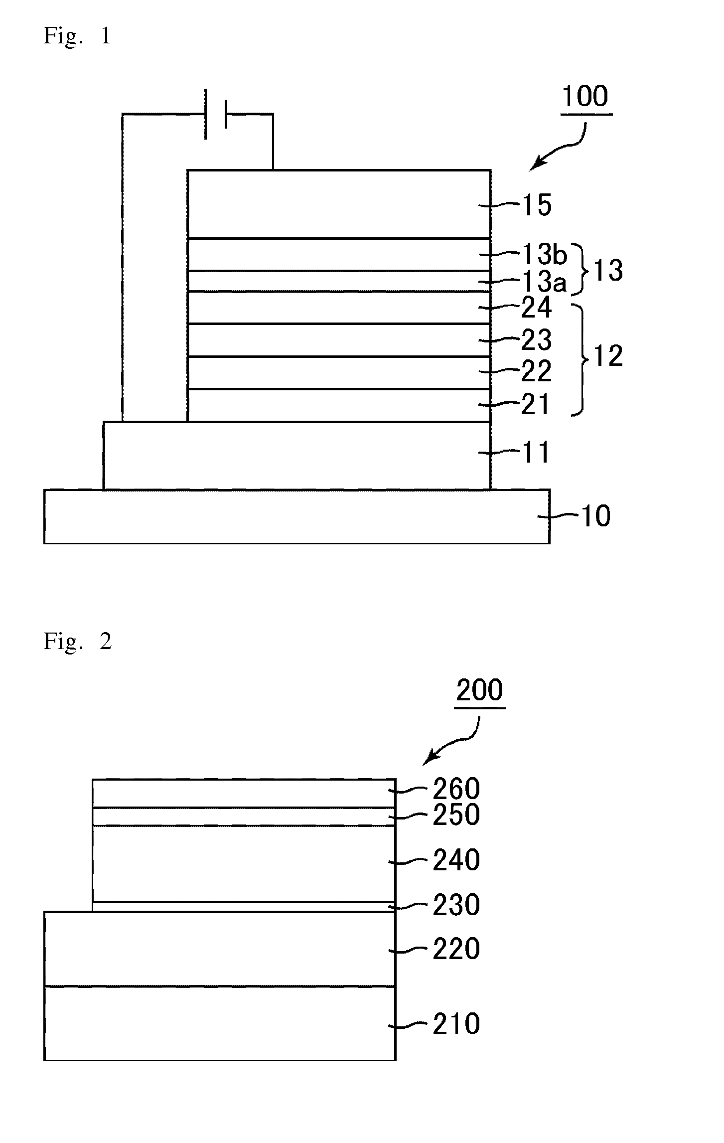
[0033]FIG. 1 is a vertical schematic cross-sectional view illustrating the structure of an organic EL display device 100 according to a first embodiment of the present invention. In FIG. 1, the organic EL display device 100 has a structure in which a substrate 10, an anode 11, an organic layer 12, an electron injection layer 13, and a cathode 15 are arranged in this order toward the viewing side. The electron injection layer 13 consists of a first electron injection layer 13a consisting of a lithium fluoride (LiF) layer and a second electron injection layer 13b made of an Mg—Ag alloy. The organic layer 12 includes a hole injection layer 21, a hole transport layer 22, a light-emitting layer 23, and an electron transport layer 24.
[0034]The substrate 10 can be, for example, a glass substrate, a resin substrate (e.g. plastic film), or a semiconductor substrate (e.g. silicon wafer). The material of the substrate 10 is not particularly limited, and may be appropriately selected according ...
PUM
 Abstract
Description
Claims
Application Information