Methods of fabricating organic thin film transistors

a thin film transistor and organic technology, applied in the field of forming banks, can solve the problems of degrading the properties of the affected electronic device, dielectric performance, and condensation failure, and achieve the effects of suppressing or eliminating adverse effects, suppressing or eliminating degradation of adjacent regions, and preventing the overflowing of organic solvents

Inactive Publication Date: 2012-05-17
SAMSUNG ELECTRONICS CO LTD
View PDF2 Cites 323 Cited by
  • Summary
  • Abstract
  • Description
  • Claims
  • Application Information

AI Technical Summary

Benefits of technology

[0011]The example embodiments, therefore, have been devised in light of the deficiencies and compromises associated with the conventional methods for fabricating such banks and the devices that incorporate such banks. Example embodiments, for example, include methods example embodiments for forming banks during the fabrication of organic electronic devices utilizing a printing technique that suppresses or eliminates adverse effects in adjacent organic electronic devices, for example, the pixel regions of adjacent devices and / or structural modules. Accordingly, methods according to example embodiments provide for the fabrication of banks sufficient to suppress or eliminate degradation of adjacent regions while still providing a degree of control with respect to the relative hydrophilicity of channel regions and / or other selected regions, thereby suppressing or preventing organic solvents from overflowing the banks.
[0012]Example embodiments also include methods for fabricating organic thin film transistor devices, for example, display drivers and / or display devices, that incorporate banks formed using one or more methods according to example embodiments for fabricating banks sufficient to suppress or eliminate degradation of adjacent regions and to provide a degree of control of the relative hydrophilicity of channel regions and / or other selected regions to improve containment of organic solvents within the banks. Example embodiments also include electronic display devices incorporating one or more such display devices that, in turn, incorporate banks formed using one or more methods according to example embodiments for fabricating banks capable of suppressing or eliminating degradation of adjacent regions by providing a degree of control of the relative hydrophilicity of channel regions and / or other active regions.

Problems solved by technology

However, the use of liquid or other flowable materials for forming and / or filling thin film patterns during the fabrication of organic electronic devices, such as display devices (e.g., electroluminescence (EL) devices and light-emitting diodes (LEDs)), in combination with conventional printing techniques can result in containment failures.
For example, the liquid material(s) may overflow the bank and spread into the pixel regions of adjacent organic electronic devices, thereby degrading the properties of the affected electronic devices.
For example, when a photoresist composition is used to form banks using an organic solvent in the fabrication of a bottom contact type or top gate type organic thin film transistor, overflow of the organic solvent can compromise the dielectric performance of adjacent organic insulating films, thereby potentially degrading the performance of the resulting organic thin film transistor.
These conventional methods, however, remain generally unsuited for fabrication processes that include bottom gate type insulating films, which are general structures of display arrays that are, in turn, used to fabricate organic devices.
In the fabrication of such devices, the organic devices are exposed to organic solvents and may be degraded as a result of this exposure.
In particular, the solvent(s) and / or solvent systems present in the compositions utilized for forming the banks, for example, the photoresist solvent(s), developing solvents and photoresist stripping compositions can degrade the underlying and / or previously patterned organic materials which, in turn, can degrade the yield, performance and / or reliability of the resulting devices.

Method used


Image

  • Methods of fabricating organic thin film transistors
  • Methods of fabricating organic thin film transistors
  • Methods of fabricating organic thin film transistors

Examples


example embodiments

DESCRIPTION OF EXAMPLE EMBODIMENTS

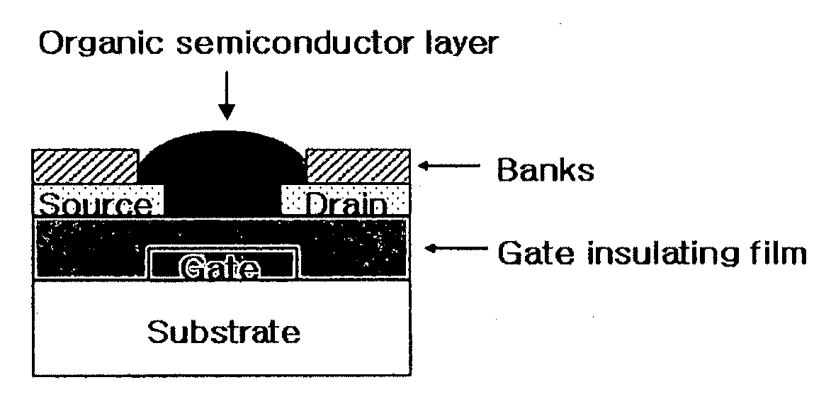
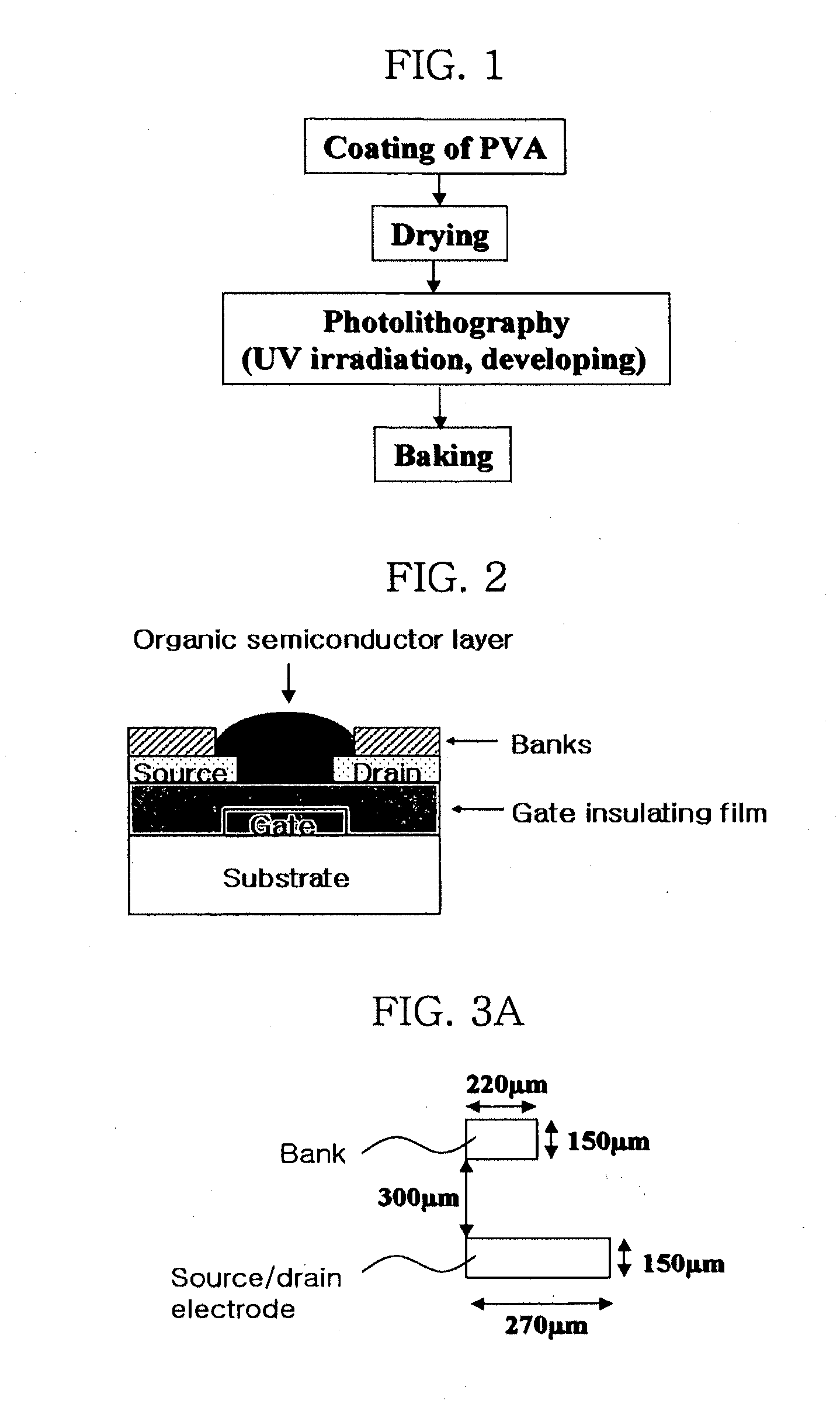
[0021]Example embodiments will now be described in detail with reference to the accompanying drawings. Example embodiments provide methods for forming banks comprising the steps of (1) coating a substrate with a water-soluble polymer solution containing a UV curing agent and a water-soluble fluorine compound, and (2) irradiating the coated water-soluble polymer solution with UV light by a photolithographic patterning process, followed by a suitable developing to form a pattern of banks on the substrate surface. FIG. 1 is a process chart schematically illustrating a method for forming banks according to one embodiment of example embodiments.

[0022]The water-soluble polymer used in the method of example embodiments has a functional group with a high affinity for water, for example, one or more groups selected from a group including —OH, —COOH, —NH2 and —CONH2, within the molecular structure and includes little or no crosslinking so that it dissolves ea...

example 1

[0050]A glass substrate was cleaned, and aluminum (Al) was deposited thereon using a sputtering technique to form a gate electrode having a thickness of about 1,500 Å. An organic gate insulating film having a thickness of about 4,000 Å was then formed on the gate electrode by spin coating at 2,000 rpm, followed by sequential baking at 70° C. for 20 minutes and 200° C. for 2 hours. As will be appreciated by those skilled in the art, the viscosity of the organic insulating material and the operation of the spin coating apparatus may be modified to produce layers having different thickness ranges.

[0051]Next, a layer of gold (Au) was deposited on the insulating film to a thickness of 700 Å using a thermal evaporation method. This conductive layer was then subjected to a photolithographic process to form an appropriate etch mask and then etched to produce an electrode pattern. For this example, the deposition was conducted under a vacuum pressure of 2×10⁻⁷ torr and achieved a deposition ...

experimental example 1

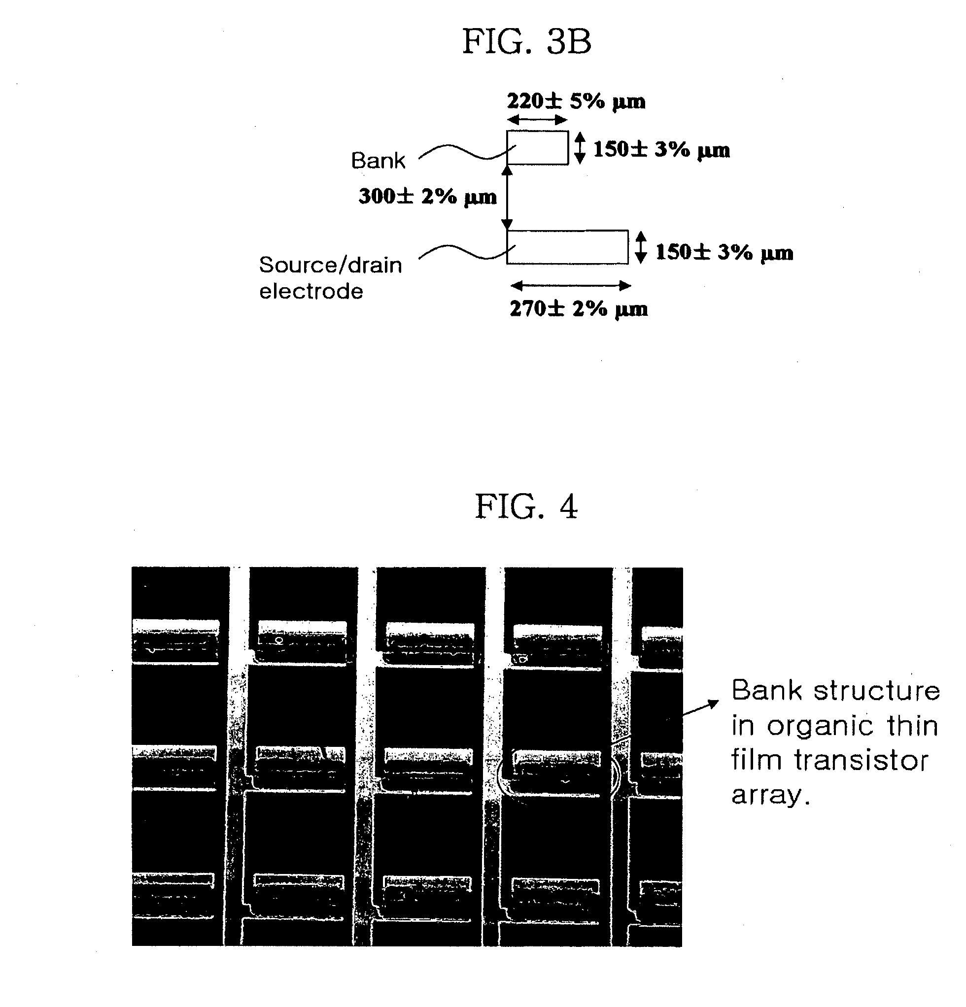
[0054]In order to evaluate the patternability of banks formed in a manner according to the example embodiments, the size of a pattern of a photomask used and that of corresponding portions of the banks formed using that photomask as detailed in Example 1 were measured using a confocal laser scanning microscope (OLYMPUS LEXT OLS3000). The results are shown in FIGS. 3A and 3B, wherein FIG. 3A shows the size of the bank and source / drain patterns of a photomask used, and FIG. 3B shows the size of the corresponding banks and source / drain structures formed using the photomask. As reflected in the close agreement between the photomask measurements and the resulting pattern measurements, the method of forming banks according to example embodiments can accurately reproduce the corresponding mask feature.

[0055]FIG. 4 shows a semiconductor array produced by depositing the semiconductor material by ink spraying after formation of the banks.


PUM


Abstract

Disclosed is a method for forming banks during the fabrication of electronic devices incorporating an organic semiconductor material that includes preparing an aqueous coating composition having at least a water-soluble polymer, a UV curing agent and a water-soluble fluorine compound. This coating composition is applied to a substrate, exposed using UV radiation and then developed using an aqueous developing composition to form the bank pattern. Because the coating composition can be developed using an aqueous composition rather than an organic solvent or solvent system, the method tends to preserve the integrity of other organic structures present on the substrate. Further, the incorporation of the fluorine compound in the aqueous solution provides a degree of control over the contact angles exhibited on the surface of the bank pattern and thereby can avoid or reduce subsequent surface treatments.

Description

PRIORITY STATEMENT[0001]This divisional application claims the benefit under 35 U.S.C. §121 of U.S. application Ser. No. 11 / 633,006, filed on Dec. 4, 2006, and claims priority under 35U.S.C. §119 to Korean Patent Application No. 10-2006-0015715, filed on Feb. 17, 2006, in the Korean Intellectual Property Office (KIPO), the entire contents of both of which are incorporated herein by reference.BACKGROUND OF EXAMPLE EMBODIMENTS[0002]1. Field[0003]Example embodiments relate to methods for forming banks for retaining liquids and other flowable materials and organic thin film transistors including such banks. More specifically, example embodiments relate to methods for forming banks during the fabrication of organic electronic devices by utilizing a printing technique wherein a mixture of a water-soluble polymer containing a UV curing agent and a water-soluble fluorine compound is used to perform the formation and surface treatment of banks substantially simultaneously, and organic thin f...

Claims


Application Information

Patent Timeline
Patent Type & Authority Applications(United States)
IPC IPC(8): H01L51/05
CPCH01L27/283H01L51/0512H01L51/0558H01L51/0005H10K19/10H10K71/135H10K10/484H10K10/462
Inventor KOO, BON WONPARK, JOON YONGHAHN, JUNG SEOKKIM, JOO YOUNGHAN, KOOK MINLEE, SANG YOON
Owner SAMSUNG ELECTRONICS CO LTD
Why Eureka
Try Eureka