Method for imaging on thin solid-state interface between two fluids

a solid-state interface and fluid technology, applied in the field of optical microscopy, can solve the problems of incompatible solid-state materials used in those contexts, difficult to bring these solid-state material surfaces, and extremely tedious to construct nano-fluidic channels, etc., to achieve high sensitivity, high contrast, and high resolution

Inactive Publication Date: 2012-05-31
TRUSTEES OF BOSTON UNIV
View PDF7 Cites 27 Cited by
  • Summary
  • Abstract
  • Description
  • Claims
  • Application Information

AI Technical Summary

Benefits of technology

[0007]Embodiments of the present invention achieve evanescent mode excitation at these solid-state membranes (carrying nanopore devices or other biological samples) by index-matched TIRFM (Total Internal Reflection Fluorescence Microscopy) between two media across these membranes. This allows for the acquisition of high resolution, high contrast and high sensitivity images of one or more biomolecules on the membrane.

Problems solved by technology

The solid state materials that have been used in those contexts, however, are incompatible with state-of-the-art optical microscopy methods, such as TIRF.
In existing techniques, it is a difficult to bring these solid state material surfaces in the evanescent field of another surface, such as a glass coverslip, and it is extremely tedious to construct the nano-fluidic channels required to bring the silicon nitride membrane and the biological sample in the TIRF evanescent field regime.
Furthermore, due to the inherent density of particles (even in the clean room environment), particulates generated during the processing of these silicon nitride chips, and limitations of temperature constraints of these silicon nitride membrane chips, sealing these nanopores with silicon nitride surfaces is a difficult task.

Method used


Image

  • Method for imaging on thin solid-state interface between two fluids
  • Method for imaging on thin solid-state interface between two fluids
  • Method for imaging on thin solid-state interface between two fluids

Examples


example 1

Sample Geometry

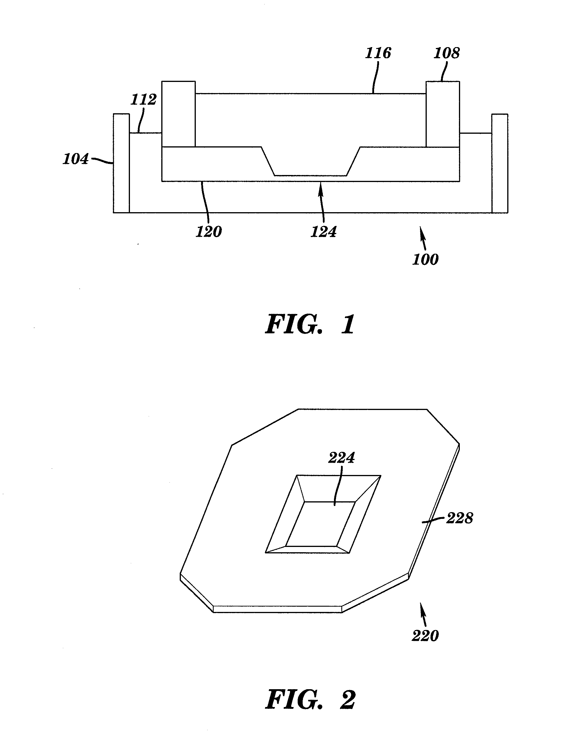
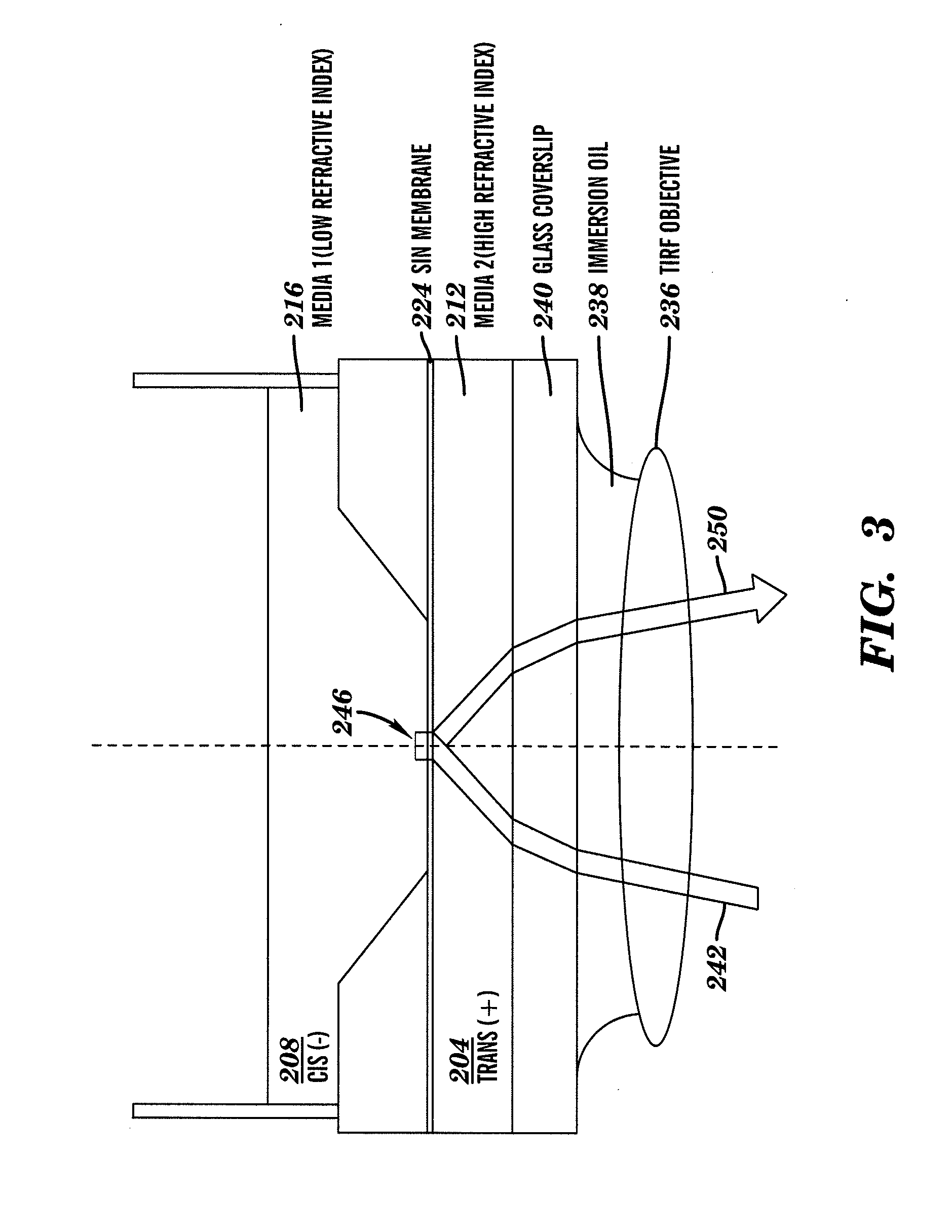
[0089]Silicon chips [5 mm×5 mm×300 μm] with a free standing 20-50 nm thick silicon nitride window [50 μm×50 μm] in the centre were made by standard photolithographic methods on LPCVD coated SiN layers on silicon wafers. A two-part PTFE / CTFE fluid cell was designed to mount these chips over a glass coverslip forming a 2-10 μm thick microchannel between the chip and glass coverslip, as shown in FIG. 3. The microchannel, trans chamber 204, was filled with fluid of a higher refractive index (70% glycerol [n=1.42]) and the cis chamber 208 was filled with a sample solution buffer in water [n=1.33].

TIRF Setup and Ray Diagram

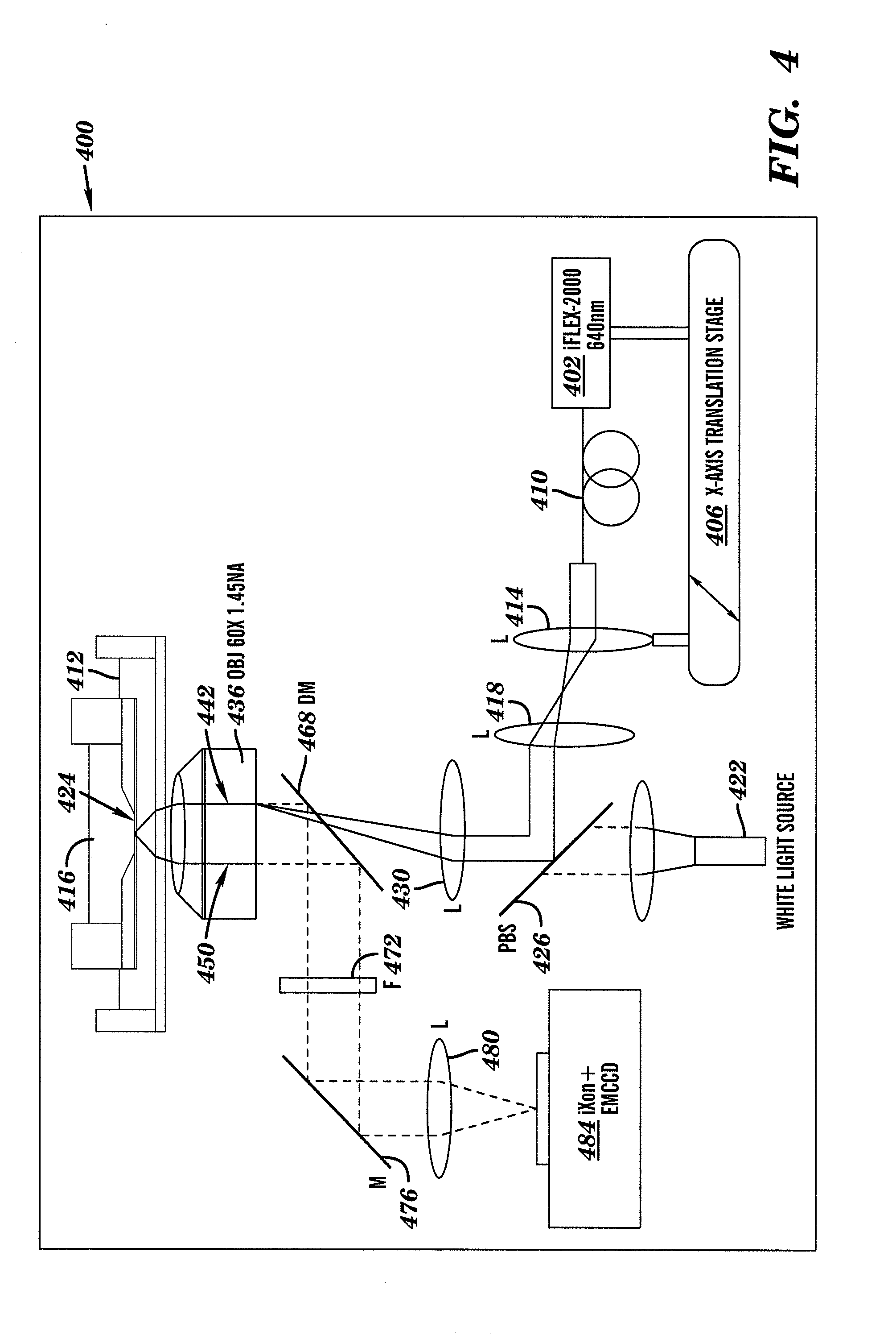
[0090]Total internal reflection [TIR] microscopy was setup as shown in FIG. 4. The laser beam size was reduced to 0.7 mm, launched into the custom designed back port of a commercially available inverted microscope (Olympus IX-71) and focused at the back focal plane of a 60× 1.45 NA oil-immersion TIRF objective via an externally mounted 200 mm focal length...

example 2

TIRF Setup

[0097]In the experiment, a silicon chip 1128 containing a free-standing SiN membrane (20×20 μm2) 1124 having a nanopore 600 was used as the interface. The silicon chip 1128 was mounted on a glass coverslip 1140, which was mounted on a custom made chlorotrifluoroethylene (CTFE polymer) fluid cell 1138 to create a micro fluidic trans chamber 1100 as shown in FIG. 11. The fluid cell 1138 included an insert 1138a holding the silicon chip 1128 and an outer cell 1138b to form the fluidic chambers. Thin layers of fast curing polydimethlysiloxane (PDMS) were used to bond the silicon chip 1128 to the CTFE insert 1138a and bond the glass coverslip 1140 to the outer cell 1138b. The fluid chamber having the insert 1138a is the cis chamber, and the space between the silicon chip 1128 and the glass coverslip 1140 is the trans chamber. The trans chamber was filled with a refractive index buffer 1112 using the inlet-outlet flow channels. For electrical measurements, a trans electrode 1140...

example 3

[0105]Simultaneous optical and electrical measurements were performed to detect the fluorophore-labeled dsDNA translocating through a 4 nm pore. Sample concentrations in this experiments was 0.1 nM-0.2 nM. FIGS. 15A-15B schematically illustrate the pore geometry, and a TEM image of an exemplary approximately 4 nm pore. A 421 bp fragment (DNA-A1647), labeled with Alexa647 fluorophores, was used by incorporation of low concentrations of amine-modified thymine bases during polymerase chain reaction (PCR) reaction followed by conjugation with the amine-reactive dye.

[0106]As shown in FIGS. 16A-16B, nine representative ion currents and their corresponding fluorescence intensity events are shown after the DNA-A1647 molecules were added to cis side of the pore (200 mV bias generating an open pore current of 4 nA; images were acquired at 1 ms integration with maximum EM gain). The nanopore location was determined as described above. The fluorescence intensity shown was extracted from a 3×3 p...


PUM

PropertyMeasurementUnit
thickaaaaaaaaaa
thickaaaaaaaaaa
thicknessaaaaaaaaaa

Abstract

Described herein is a fluid cell for an optical microscopy tool having a solid state membrane having a first side and a second, opposing side; a first fluid chamber comprising a first fluid having a first refractive index located on the first side of the membrane; and, a second fluid chamber comprising a second fluid having a second refractive index located on the second side of the membrane, the second refractive index being different than the first refractive index. Also described herein is a method for imaging a single biomolecule, the method including generating a field of evanescent illumination at a solid state membrane between a first fluid and a second fluid having different refractive indexes; and detecting light emitted by optical detectors linked to the single biomolecules at the solid state membrane.

Description

CROSS-REFERENCE TO RELATED APPLICATIONS[0001]This application is a continuation of International Application No. PCT / US2010 / 028845, filed Mar. 26, 2010, which claims the benefit of priority to U.S. Provisional Application No. 61 / 211,260, filed Mar. 26, 2009, the entire disclosures of which are hereby incorporated by reference.GOVERNMENT SUPPORT[0002]This invention was made with Government Support under Contract No. HG-004128 awarded by the National Institutes of Health. The Government has certain rights in the invention.FIELD OF THE INVENTION[0003]The present invention relates to the field of optical microscopy. In particular, the invention utilizes a thin solid-state interface between two fluids for improved imaging of biomolecules.BACKGROUND[0004]The completion of the first reference human genome sequence has marked the commencement of an era in which genomic variations directly impact drug discovery and medical therapy. This new paradigm has created an imminent need for inexpensi...

Claims


Application Information

Patent Timeline
Patent Type & Authority Applications(United States)
IPC IPC(8): G01N21/75B01L3/00B82Y15/00
CPCG01N21/0303G02B21/16G02B21/0088G01N21/648G01N2021/6482G01N33/483G01N21/00G01N35/00
Inventor SONI, GAUTAM V.MELLER, AMIT
Owner TRUSTEES OF BOSTON UNIV
Why Eureka
Try Eureka