Ambipolar polymeric semiconductor materials and organic electronic devices

a semiconductor material and polymer technology, applied in semiconductor devices, solid-state devices, thermoelectric devices, etc., can solve problems such as poor performance, achieve high electron and hole mobilities, efficient electron injection and transport, and low lumo energy level

Active Publication Date: 2012-06-21
AGENCY FOR SCI TECH & RES
View PDF0 Cites 32 Cited by
  • Summary
  • Abstract
  • Description
  • Claims
  • Application Information

AI Technical Summary

Benefits of technology

[0011]The compounds of the invention incorporate alternating blocks of electron accepting groups and electron donating groups. The compounds are polymers comprising a repeating unit that is based on a core planar acceptor moiety that is deficient in electrons and can provide electron transport properties and a donor moiety that is rich in electrons to provide hole transport properties. An additional acceptor moiety contributes, along with the core acceptor group, provision of a low LUMO energy level for efficient electron injection and transport. The donor and acceptor groups provide balanced electron and hole transport.
[0012]The compounds of the invention may exhibit high, well-balanced electron and hole mobilities. Thus, the compounds may be useful as a single-component ambipolar semiconductor material for inclusion in organic electronic devices, including in organic thin film transistors.

Problems solved by technology

However, the use of unipolar p-type and n-type organic semiconductors for bilayered (i) or mixed layered (ii) ambipolar OTFTs requires complicated fabrication procedures or such devices have shown poor performance.

Method used


Image

  • Ambipolar polymeric semiconductor materials and organic electronic devices
  • Ambipolar polymeric semiconductor materials and organic electronic devices
  • Ambipolar polymeric semiconductor materials and organic electronic devices

Examples


example 1

Synthesis of Polymer (1)

[0110]Polymer (1) was synthesized according to Scheme 1 as set out below, based on the following synthetic steps: i) diisopropylsuccinate / t-C5H11OK / 2-methyl-2-butanol / 120° C.; ii) 2-octyl-1-dodecyl bromide / K2CO3 / DMF / 130° C.; iii) NBS / chloroform; v) Pd(dppf)Cl2 / KOAc / 1,4-dioxane; vi) Pd(PPh3)4 / Aliquat 336 / 2M K2CO3 / toluene.

[0111](i) Synthesis of 2,5-dihydro-1,4-dioxo-3,6-dithienylpyrrolo [3,4-c]-pyrrole (1-2): Sodium metal (6.90 g, 0.30 mol) was added to 100 ml t-amyl alcohol and a small amount of iron (III) chloride (100 mg) was added. The mixture was stirred vigorously for 2 hr at 105° C. until the sodium dissolved. The solution was cooled to 85° C. and 2-thiophenecarbonitrile (22.0 g, 0.2 mol) was added. Diisopropyl succinate (16.6 g, 0.08 mol) dissolved in 10 ml of t-amyl alcohol was added dropwise to the reaction mixture over 1 hr at 85° C. The reaction mixture was stirred at this temperature for 12 hrs, then cooled to 50° C., diluted with 100 ml of methano...

example 2

Synthesis of Polymer (2)

[0116]Polymer (2) was synthesized according to Scheme 2 as set out below, based on the following synthetic steps: i) 2-butyl-1-octanol, H2SO4, 98%; ii) AgNO3 / KF / Pd(PhCN)Cl2 / DMSO, 62%; iii) 2-tributylstannylthiophene, Pd2dba3 / P(o-tolyl)3 / toluene, 75%; iv) 2 eq. NBS, 97%; v) Pd(PPh3)4, 2M Na2CO3, 2,1,3-Benzothiadiazole-4,7-bis(boronic acid pinacol ester), toluene, reflux, 24 hr, 56%.

[0117](i) Synthesis of 2-butyl-1-ocatyl 2-bromo-3-thiophenecarboxylate: In a 500 ml, round-bottomed flask equipped with a Dean-Stark apparatus and a water condenser were placed 4.5 g of 2-bromo-3-thiophenecarboxylic acid (21.7 mmol), 9.32 g (50 mmol) of 2-butyl-1-octanol, 0.44 g (4.8 mmol) of conc. H2SO4, and 100 ml of toluene. The mixture was heated under reflux for 24 hr. The mixture was'cooled to room temperature and then dissolved in ethyl acetate (100 ml) and the solution was washed with dilute sodium bicarbonate (twice) and water (twice), and then dried over MgSO4, and the sol...

example 3

Fabrication of Devices with Polymer (1)

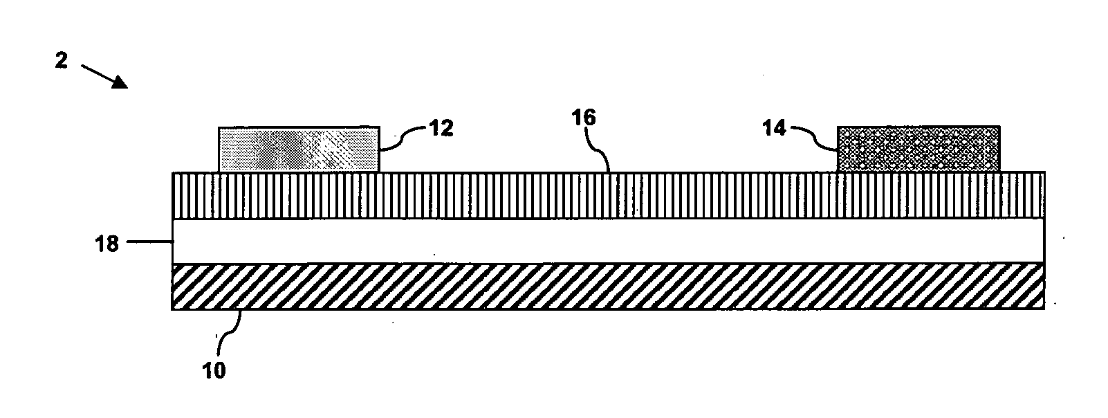
[0122]Device Fabrication

[0123]Top contact / bottom gate OTFT devices were fabricated as follows.

[0124](i) Substrate Preparation: p+-Si (or n+-Si) / SiO2 substrates were used for OTFT fabrication where p+-Si (or n+-Si) and SiO2 work as gate contact and gate dielectric, respectively. Substrates were subject to routine cleaning using ultrasonication in acetone, methanol and de-ionized water. The cleaned wafers were dried under a nitrogen flow and heated at 100° C. for 5 minutes and then were subjected to UV-ozone treatment for 20 minutes.

[0125](ii) Self-assembled monolayer (SAM): p+-Si (or n+-Si) / SiO2 substrates were kept in a desiccator with few drops of octyltricholorosilane (OTS). A vacuum was applied to the desiccator for 3 minutes and then the desiccator was placed in an oven at 110° C. for three hours. p+-Si (or n+-Si) / SiO2 substrates were then removed from desiccators, thoroughly rinsed with isopropanol and dried under a nitrogen flow.

[0126](ii...


PUM

PropertyMeasurementUnit
electron mobilityaaaaaaaaaa
electron mobilitiesaaaaaaaaaa
electron mobilityaaaaaaaaaa

Abstract

There is provided compounds of formula I, ambipolar semiconductor material derived from such compounds and devices comprising such ambipolar semiconductor material.
[Da-Acore-Db-Ac-]n  (I)

Description

CROSS-REFERENCE TO RELATED APPLICATION[0001]This application claims benefit of, and priority from, U.S. provisional patent application No. 61 / 272,182, filed on Aug. 28, 2009, the contents of which are hereby incorporated herein by reference.FIELD OF THE INVENTION[0002]The present invention relates to organic compounds, ambipolar semiconductor material derived from such compounds and devices comprising such ambipolar semiconductor material.BACKGROUND OF THE INVENTION[0003]There has been much development of organic compounds as semiconductor materials. In particular, high performance unipolar p-type and n-type polymer semiconductors have been developed in recent years, having hole and electron mobility, respectively, approaching 1 cm2 / V·s. Polymer semiconductors with high transport mobility in thin film transistors are useful in many applications, including displays and RFIDs.[0004]Ambipolar organic thin film transistors capable of conducting both holes and electrons in p- and n-chann...

Claims


Application Information

Patent Timeline
Patent Type & Authority Applications(United States)
IPC IPC(8): H01L51/54C08G75/06C08G73/06
CPCH01L51/0545H01L51/0036H10K85/113H10K10/466
Inventor SONAR, PRASHANTSINGH, SINGARENDRA P.SOH, MUI SIANGLI, YUNING
Owner AGENCY FOR SCI TECH & RES
Why Eureka
Try Eureka