Epitaxial substrate and method for manufacturing epitaxial substrate

a technology of epitaxial substrate and nitride, which is applied in the direction of crystal growth process, polycrystalline material growth, chemically reactive gas growth, etc., can solve the problems of high reliability and cost reduction, hinder the formation of good nitride, and difficult to form a good nitride film on a silicon substrate. , to achieve the effect of good crystal quality, good surface flatness and low dislocation

Active Publication Date: 2012-06-28
NGK INSULATORS LTD
View PDF2 Cites 14 Cited by
  • Summary
  • Abstract
  • Description
  • Claims
  • Application Information

AI Technical Summary

Benefits of technology

[0045]In the first to twenty-fourth aspects of the present invention, the compressive strain exists in the buffer layer. Accordingly, a tensile stress caused by a difference in a thermal expansion coefficient between silicon and a group-III nitride is cancelled by the compressive strain. Therefore, a crack-free epitaxial substrate having a small amount of warping and an excellent crystal quality can be obtained even when a silicon substrate is used as the base substrate.
[0046]Particularly, in the ninth to eleventh aspects and nineteenth to twenty-first aspects, a crack-free epitaxial substrate having a small amount of warping and excellent breakdown voltage properties is achieved.
[0047]Particularly, in the thirteenth and twenty-third aspects, an epitaxial substrate having a further smaller amount of warping is achieved.
[0048]Particularly, in the fourteenth and twenty-fourth aspects; the buffer layer is provided on the base layer having a low dislocation and an excellent surface flatness. Accordingly, the buffer layer, the crystal layer, and the like, have good crystal quality. On the other hand, an accumulation of strain energy in the second base layer is suppressed. Therefore, the effect of canceling the tensile stress exerted by the compressive strain existing in the buffer layer is not hindered by any accumulation of strain energy in the base layer.

Problems solved by technology

The HEMT device and the HEMT-device substrate involve various problems including problems concerning improvement of the performance such as increasing the power density and efficiency, problems concerning improvement of the functionality such as a normally-off operation, fundamental problems concerning a high reliability and cost reduction, and the like.
However, it is known that forming a nitride film of good quality on a silicon substrate is very difficult as compared with a case of using a sapphire substrate or a SiC substrate, for the following reasons.
In other words, this is a factor that hinders the formation of a good nitride epitaxial film having a low dislocation density and a flat surface.
As a result, it is likely that cracking occurs in a film surface and large warping occurs in the substrate.
However, the resulting GaN film never has a better crystal quality as compared with a case of using SiC or sapphire for the base substrate.
Therefore, preparing an electronic device such as a HEMT using the conventional techniques involves problems of a low electron mobility, a leakage current during the off-time, and a low breakdown voltage.
Furthermore, in the method disclosed in the Patent Document 4, large convex warping is intentionally caused in the course of the device preparation.
This may cause cracking in the course of the device preparation, depending on conditions under which the layers are formed.

Method used


Image

  • Epitaxial substrate and method for manufacturing epitaxial substrate
  • Epitaxial substrate and method for manufacturing epitaxial substrate
  • Epitaxial substrate and method for manufacturing epitaxial substrate

Examples


example 1

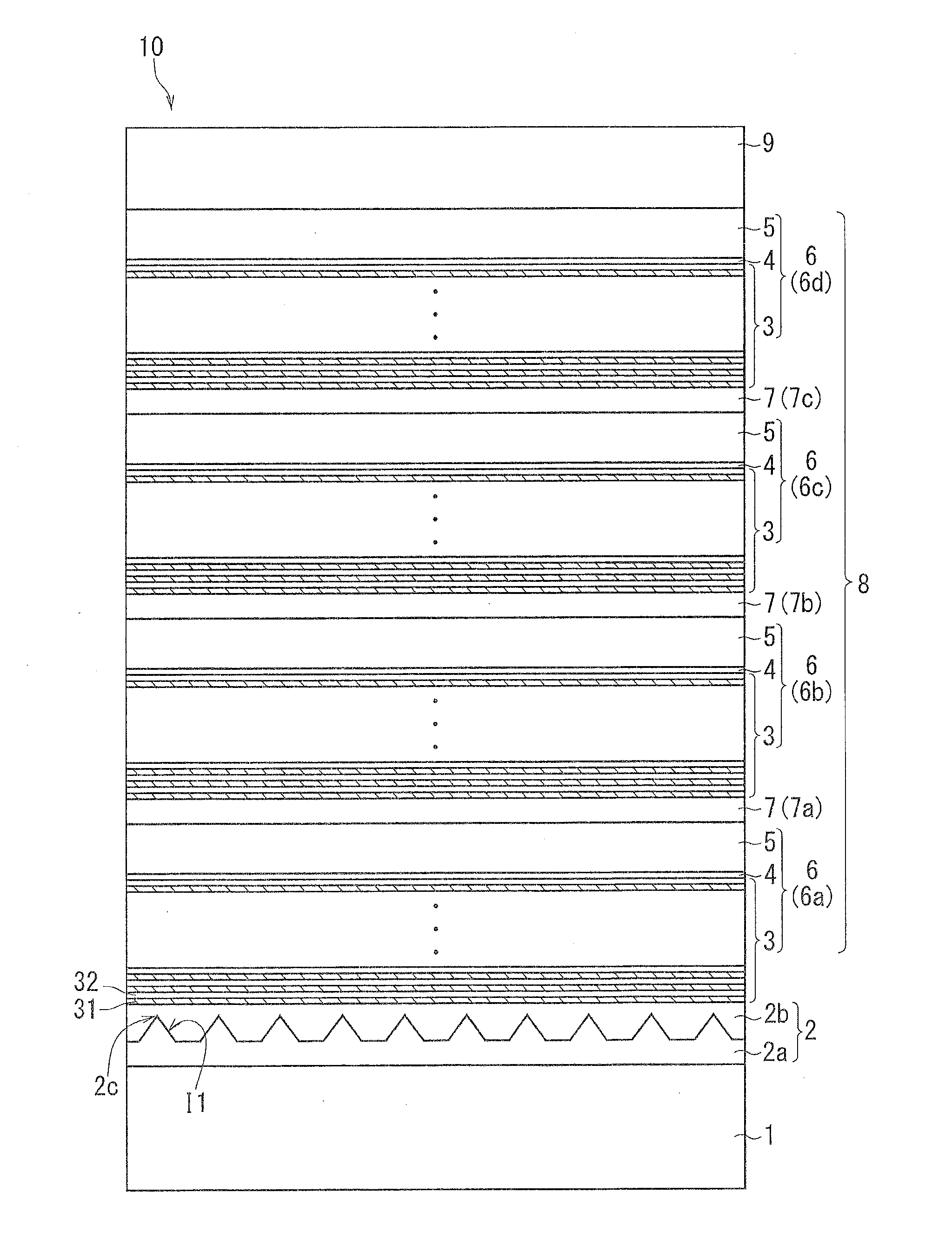
[0147]In this example, the values of D, E, n, and K were variously changed and thereby 27 kinds of epitaxial substrates 10 (specimens a-1 to a-27) were prepared which were different from one another in terms of the configuration of the buffer layer 8. Then, the presence or absence of occurrence of cracking was evaluated, and the amount of warping was measured. In any specimen, A=C=5 nm and B=15 nm. FIG. 4 is a diagram showing a list of the configuration of each layer, the presence or absence of occurrence of cracking, and the amount of warping, with respect to each epitaxial substrate 10.

[0148]Until the formation of the second base layer 2b, the same procedure was performed for any of the specimens. A (111) plane single crystal silicon wafer (hereinafter, a silicon wafer) of 4 inch having a p-type conductivity and having a substrate thickness of 525 μm was prepared as the base substrate 1. The prepared silicon wafer was subjected to dilute hydrofluoric acid cleaning using dilute hyd...

example 2

[0160]In this example, the values of x, y, D, E, n, and K were variously changed and thereby 32 kinds of epitaxial substrates 10 (specimens b-1 to b-35) in which the second unit layer 32 and the first intermediate layer 5 contained Al were prepared in the same procedure as in the example 1. Then, the presence or absence of occurrence of cracking was evaluated, the amount of warping was measured, and the breakdown voltage was measured. In any specimen, A=C=5 nm and B=15 nm.

[0161]FIG. 5 is a diagram showing a list of the configuration of each layer, the presence or absence of occurrence of cracking, the amount of warping, and the breakdown voltage, with respect to each epitaxial substrate 10. In FIG. 5, for comparison, the layer configurations and the evaluation results with respect to the specimens a-7 to a-9 of the example 1 in which the Al mole fraction is zero are also shown.

[0162]As shown in FIG. 5, no cracking occurred in the specimens b-1 to b-33 while cracking occurred at 20 m...

example 3

[0167]In this example, 16 kinds of epitaxial substrates 10 (specimens c-1 to c-16) in which the thickness of the termination layer 4 is larger than the thickness of the first unit layer 31 were prepared in the same procedure as in the example 1. Then, the presence or absence of occurrence of cracking was evaluated, the amount of warping was measured, and the breakdown voltage was measured. In any specimen, A=C=5 nm and B=15 nm.

[0168]FIG. 7 is a diagram showing a list of the configuration of each layer, the presence or absence of occurrence of cracking, the amount of warping, and the breakdown voltage, with respect to each epitaxial substrate 10.

[0169]As shown in FIG. 7, occurrence of cracking was not observed in all the specimens c-1 to c-16. In any specimen, the amount of warping was suppressed to about 70 μm or less which is far below 100 μm. Additionally, comparing results shown in FIG. 7 with the results shown in FIG. 5 that are for the specimens having the same configuration ex...


PUM


Abstract

Provided is a crack-free epitaxial substrate having a small amount of warping, in which a silicon substrate is used as a base substrate. The epitaxial substrate includes a (111) single crystal Si substrate, a buffer layer, and a crystal layer. The buffer layer is formed of a first lamination unit and a second lamination unit being alternately laminated. The first lamination unit includes a composition modulation layer and a first intermediate layer. The composition modulation layer is formed of a first unit layer and a second unit layer having different compositions being alternately and repeatedly laminated so that a compressive strain exists therein. The first intermediate layer enhances the compressive strain existing in the composition modulation layer. The second lamination unit is a second intermediate layer that is substantially strain-free.

Description

TECHNICAL FIELD[0001]The present invention relates to an epitaxial substrate for use in a semiconductor device, and particularly to an epitaxial substrate made of a group-III nitride.BACKGROUND ART[0002]A nitride semiconductor is attracting attention as a semiconductor material for a light-emitting device such as a LED or a LD and for a high-frequency / high-power electronic device such as a HEMT, because the nitride semiconductor has a wide band gap of direct transition type and the breakdown electric field and the saturation electron velocity thereof are high. For example, a HEMT (high electron mobility transistor) device in which a barrier layer made of AlGaN and a channel layer made of GaN are laminated takes advantage of the feature that causes a high-concentration two-dimensional electron gas (2DEG) to occur in a lamination interface (hetero interface) due to the large polarization effect (a spontaneous polarization effect and a piezo polarization effect) specific to a nitride m...

Claims


Application Information

Patent Timeline
Patent Type & Authority Applications(United States)
IPC IPC(8): H01L29/205H01L21/20H01L29/04
CPCC30B25/186C30B29/403H01L21/02381H01L21/02458H01L29/7787H01L21/0254H01L29/045H01L29/2003H01L29/205H01L21/02507
Inventor MIYOSHI, MAKOTOSUMIYA, SHIGEAKIICHIMURA, MIKIYAMAEHARA, SOTATANAKA, MITSUHIRO
Owner NGK INSULATORS LTD
Why Eureka
Try Eureka