

Memory device and semiconductor device
- Summary
- Abstract
- Description
- Claims
- Application Information
AI Technical Summary
Benefits of technology
Problems solved by technology
Method used
Image

Examples
embodiment 1
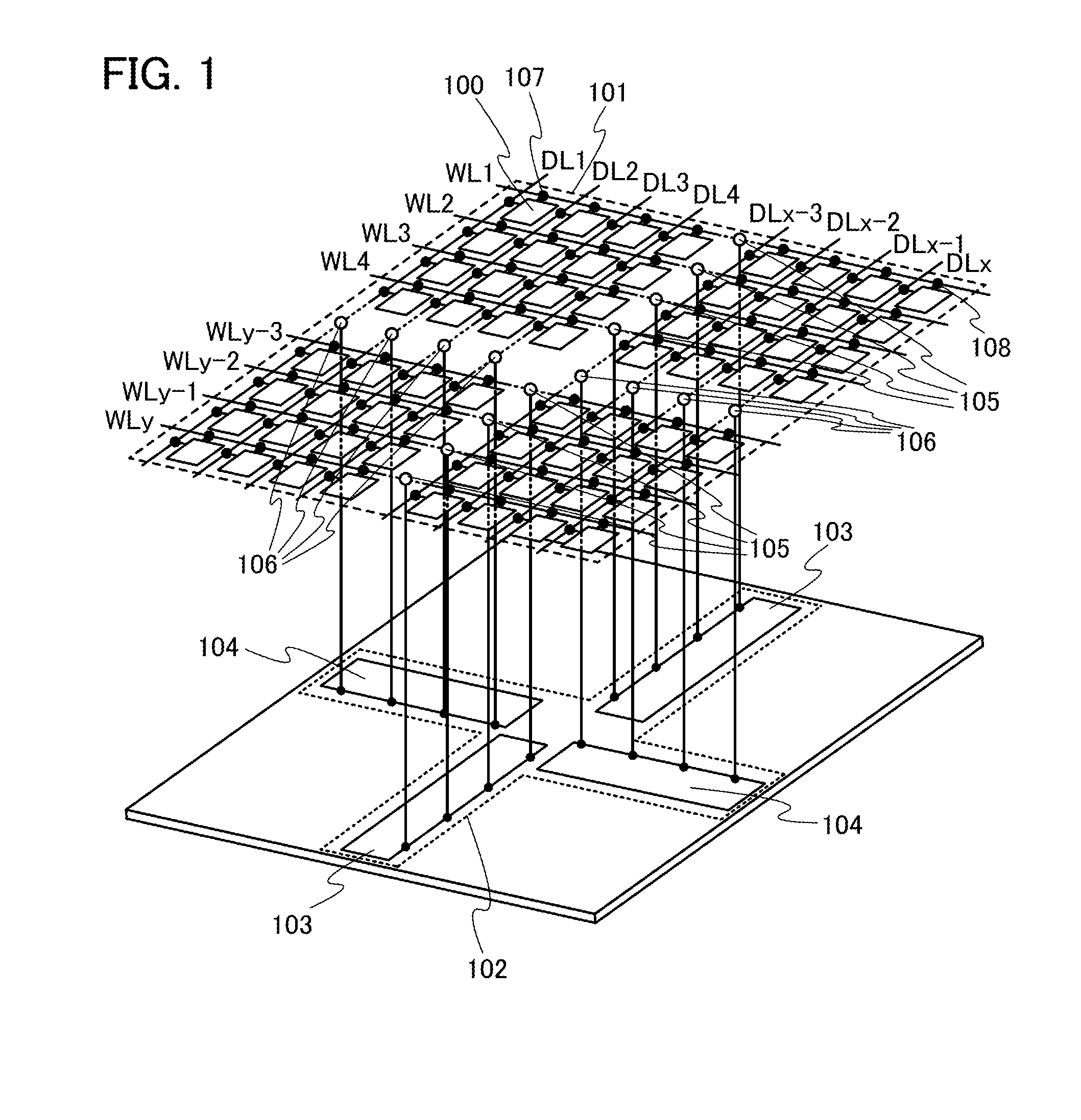
[0050]FIG. 1 illustrates the structure of the memory device according to an embodiment of the present invention. The memory device illustrated in FIG. 1 includes a cell array 101 in which a plurality of memory cells 100 are arranged in matrix and a driver circuit 102 provided below the cell array 101.
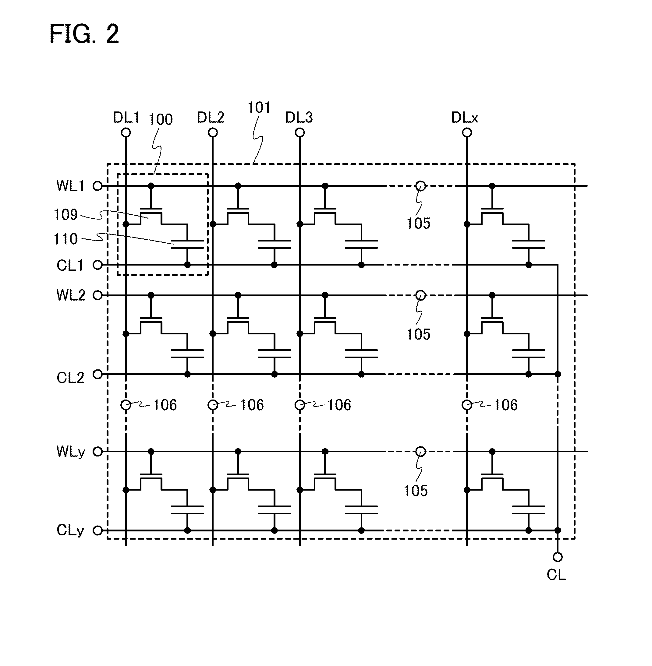
[0051]Further, in the cell array 101, a plurality of wirings for supplying potentials to the memory cell 100 are provided. Specifically, a plurality of word lines WL and a plurality of data lines DL are provided for the cell array 101 illustrated in FIG. 1.
[0052]Note that the number of the wirings can be determined by the number of the memory cells 100 and arrangement of the memory cells 100 in the cell array 101. Specifically, FIG. 1 illustrates an example in the case where the memory cells 100 in x rows and y columns are connected in matrix and the word lines WL1 to WLy and the data lines DL1 to DLx are arranged in the cell array 101. Further, each of the memory cells 100 is connected...
embodiment 2
[0113]An example of a specific structure of the driver circuit in the memory device will be described.
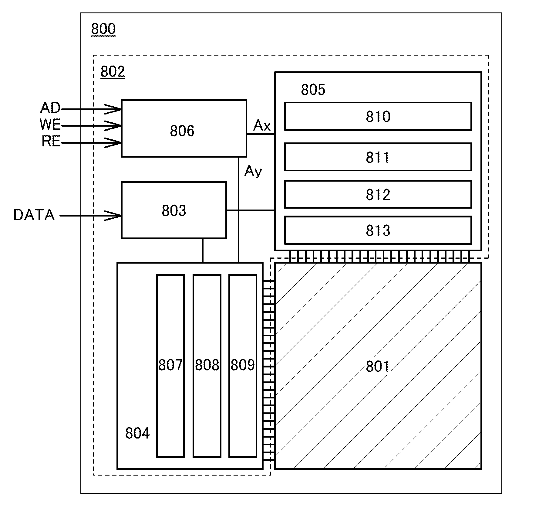
[0114]FIG. 4 illustrates a block diagram of a specific structure of the memory device as an example. In the block diagram in FIG. 4, circuits in the memory device are classified in accordance with their functions and illustrated as separate blocks; however, it is difficult to classify actual circuits according to their functions completely and one circuit may have a plurality of functions.
[0115]A memory device 800 illustrated in FIG. 4 includes a cell array 801 and a driver circuit 802. The driver circuit 802 includes an input-output buffer 803; a word line driver circuit 804 configured to control the potential of a word line; a data line driver circuit 805 configured to control writing and reading of data to / from a memory cell; and a control circuit 806 configured to control operations of the input-output buffer 803, the word line driver circuit 804, and the data line driver circui...
embodiment 3
[0125]Next, a specific structural example of the reading circuit will be described.
[0126]The levels of potentials read from the cell array are determined in accordance with data written to the memory cells. Accordingly, ideally, potentials having the same level should be read from the plurality of memory cells when data with the same digital value is stored in the plurality of memory cells. However, practically, there is a case where the characteristics of as capacitors and transistors which function as switching elements vary among the memory cells. In that case, the potentials actually read vary even when all of the data to be read have the same digital value, so that the levels of the potentials can be widely distributed. However, even when potentials read from the cell array vary slightly, a reading circuit can generate a signal including accurate data and having an amplitude and a waveform processed in accordance with a desired specification.
[0127]FIG. 5 is a circuit diagram il...
PUM
 Abstract
Description
Claims
Application Information