
Photoelectric conversion device and electronic apparatus

a conversion device and photoelectric technology, applied in the direction of photovoltaic energy generation, electrical equipment, semiconductor devices, etc., can solve the problems of difficult to reduce the leakage of current (dark current), cis thin films are liable to be damaged, and the leakage of current is difficult to reduce, so as to achieve stable photoelectric conversion and high electro-optic characteristics

Active Publication Date: 2012-08-16
SEIKO EPSON CORP
View PDF7 Cites 10 Cited by
  • Summary
  • Abstract
  • Description
  • Claims
  • Application Information

AI Technical Summary

Benefits of technology

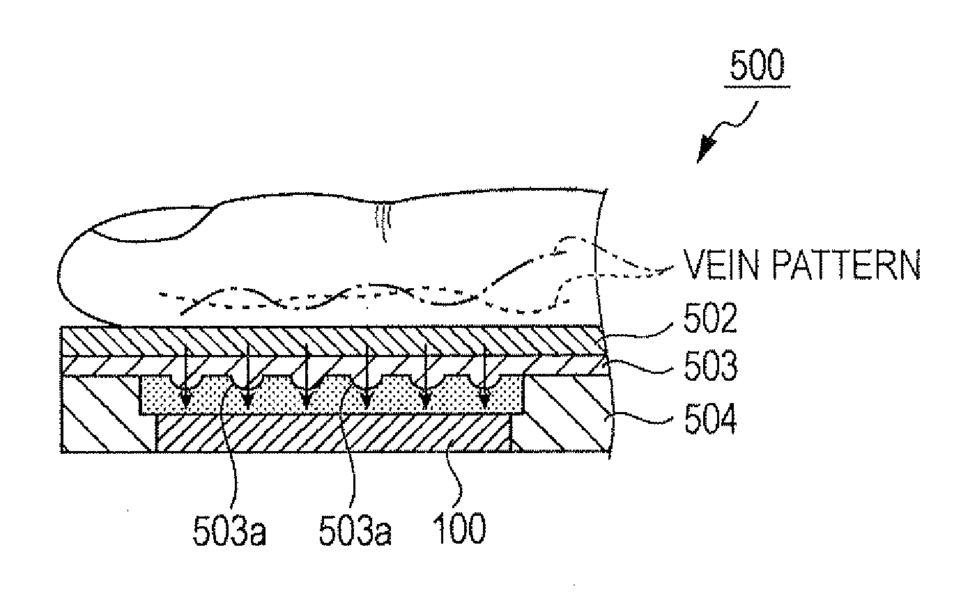
The present invention provides a photoelectric conversion device that includes a light absorption layer, a window layer, and an amorphous oxide semiconductor layer. The amorphous oxide semiconductor layer acts as a buffer layer with higher resistance than the CdS film, reducing drift current and dark current. The device also has a larger band gap than the light absorption layer, reducing loss of light. The amorphous oxide semiconductor layer can contain a Group 12 element and a Group 13 element to increase its band gap. The device can be used as a photosensor in electronic apparatuses.

Problems solved by technology

On the other hand, CIS thin films are liable to be damaged when being formed for a photodetector, and the damaged CIS film undesirably causes leakage of current.
While the solid state image pickup device produced by the method disclosed in International Publication No. 2008 / 093834 is effective in reducing leakage of current that may occur when a forward bias is applied, however, it is difficult to reduce leakage of current (dark current) that may occur when a reverse bias is applied.
However, if the CdS film has a crystal defect, leakage of current occurs undesirably at the position of the crystal defect.

Method used


Image

  • Photoelectric conversion device and electronic apparatus
  • Photoelectric conversion device and electronic apparatus
  • Photoelectric conversion device and electronic apparatus

Examples


example

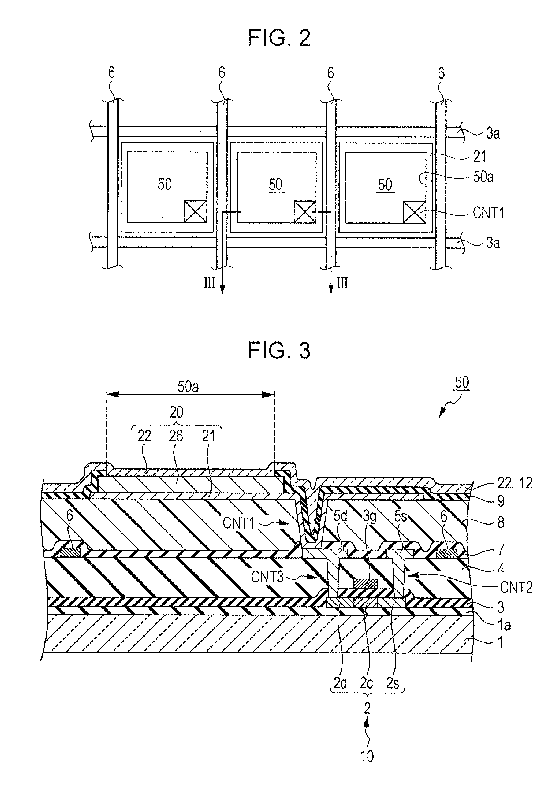
[0056]The first electrode 21 may be formed of a metal such as Mo (molybdenum), Nb (niobium), Ta (tantalum) or W (tungsten) by sputtering. In the Example, the first electrode 21 was formed on Mo to a thickness of about 400 nm.

[0057]The p-type compound semiconductor film acting as the light absorption layer 23 may be formed of a CIS (for example, CuInSe2 or CuInGaSe) thin film having a chalcopyrite structure. In the Example, the light absorption layer 23 was formed of CuInSe2 to a thickness of about 1.5 μ (1500 nm) by sputtering.

[0058]In the CIS thin film of the light absorption layer 23 having a composition Cu(Inx, Ga1-x)Se2 (0≦x≦1), the wavelength band of light that the light absorption layer 23 can absorb can be expanded up to about 1300 nm or the near-infrared region by altering the composition from Cu(InGa)Se2 to CuInSe2.

[0059]It is preferable that the amorphous oxide semiconductor layer 24 contain Group 12 and Group 13 elements, which are defined by International Union of Pure a...

modification 1

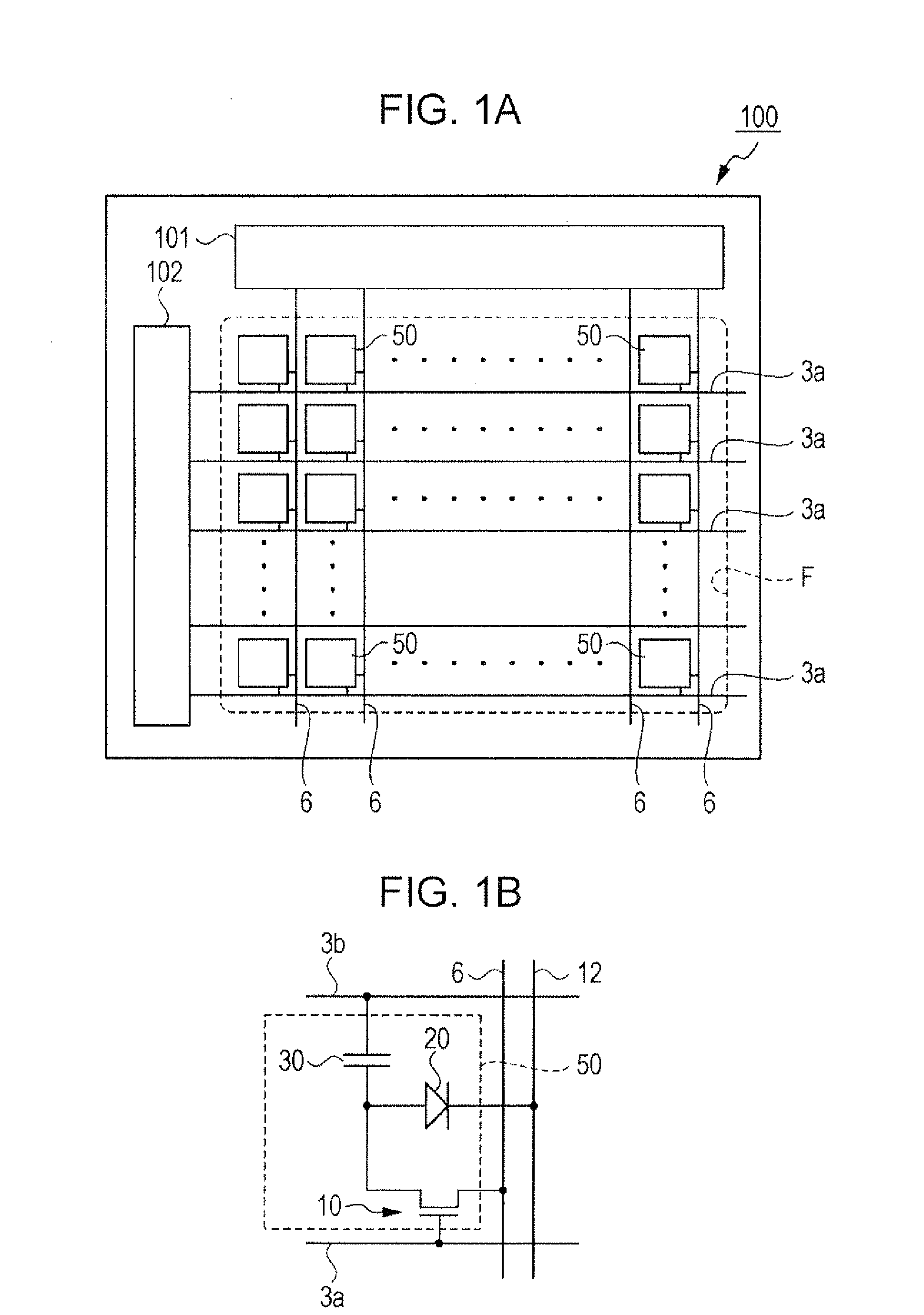
[0082]In the image sensor 100, the electrical configuration and connection of the photosensors 50 are not limited to those disclosed in the above embodiment. For example, the photodiode 20 may be electrically connected to the gate electrode 3g of the corresponding TFT 10 so that light received by the photosensor 20 can be detected as a change in voltage or current between the source electrode 5s and the drain electrode 5d.

modification 2

[0083]The shape in plan view of the light-receiving region 50a of the photosensor 50 is not limited to that disclosed in the above embodiment. For example, the light-receiving region 50a may be in a round or oval form, or in a polygonal form, such as triangular, rectangular or pentagonal form.


PUM


Abstract

A photoelectric conversion device includes circuit portions disposed on a substrate, a first electrode electrically connected to one of the circuit portions, an optically transparent second electrode opposing the first electrode, and a photoelectric conversion portion disposed between the first electrode and the second electrode. The photoelectric conversion portion has a multilayer structure including a light absorption layer made of a p-type compound semiconductor film having a chalcopyrite structure, an amorphous oxide semiconductor layer, and a window layer made of an n-type semiconductor film.

Description

[0001]This application claims priority to JP 2011-030535, filed Feb. 16, 2011. The disclosure of the priority application is hereby incorporated by reference herein in its entirety.BACKGROUND[0002]1. Technical Field[0003]The present invention relates to a photoelectric conversion device that converts light energy into electrical energy, and the electronic apparatus including the photoelectric conversion device.[0004]2. Related Art[0005]A solar cell including a light absorption layer is a typical example of photoelectric conversion devices. The light absorption layer may be made of a CIS thin film, such as a CuInSe2 or CuInGaSe film, which is an p-type semiconductor film having a chalcopyrite structure. CIS thin films have high photosensitivity to light over a wide range of wavelengths from visible light to near-infrared light, and are accordingly expected to be used in photodetectors. On the other hand, CIS thin films are liable to be damaged when being formed for a photodetector, a...

Claims


Application Information

Patent Timeline
Patent Type & Authority Applications(United States)
IPC IPC(8): H01L31/0264H01L31/0376
CPCH01L27/14645H01L27/14632Y02E10/541H01L31/04H01L31/06
Inventor HATTORI, YASUNORIMATSUMOTO, TOMOTAKAEGUCHI, TSUKASA
Owner SEIKO EPSON CORP
Learn More