Back Contact Solar Cell with Organic Semiconductor Heterojunctions

a solar cell and organic semiconductor technology, applied in the field of solar cell fabrication, can solve the problems of low forward gain and reverse gain, high forward gain and low forward gain, and the limitation of the cell ar, so as to reduce the surface recombination at the a-si/n-type organic semiconductor interface, the interface quality is good, and the surface recombination is reduced

Inactive Publication Date: 2012-08-23
SHARP LAB OF AMERICA INC SLA
View PDF9 Cites 30 Cited by
  • Summary
  • Abstract
  • Description
  • Claims
  • Application Information

AI Technical Summary

Benefits of technology

[0027]Disclosed herein is a heterojunction back contact solar cell with heterojunctions formed between organic semiconductors, such as polymers, and silicon (Si) at both the n+and p+contacts. In order to have high interface quality, a thin intrinsic amorphous silicon layer is inserted between the silicon and organic semiconductor because of the good interface quality between hydrogenated amorphous silicon (a-Si:H) and single-crystal silicon (c-Si). The valance band discontinuity at the a-Si:H/c-Si

Problems solved by technology

The limitations of this cell are
(d) rear surface recombination loss due to the low Al back surface passivation quality.
When a heterojunction is used as the base-emitter junction of a bipolar junction transistor, extremely high forward gain and low reverse gain result.
While several papers discuss a double heter

Method used


Image

  • Back Contact Solar Cell with Organic Semiconductor Heterojunctions
  • Back Contact Solar Cell with Organic Semiconductor Heterojunctions
  • Back Contact Solar Cell with Organic Semiconductor Heterojunctions

Examples


Embodiment Construction

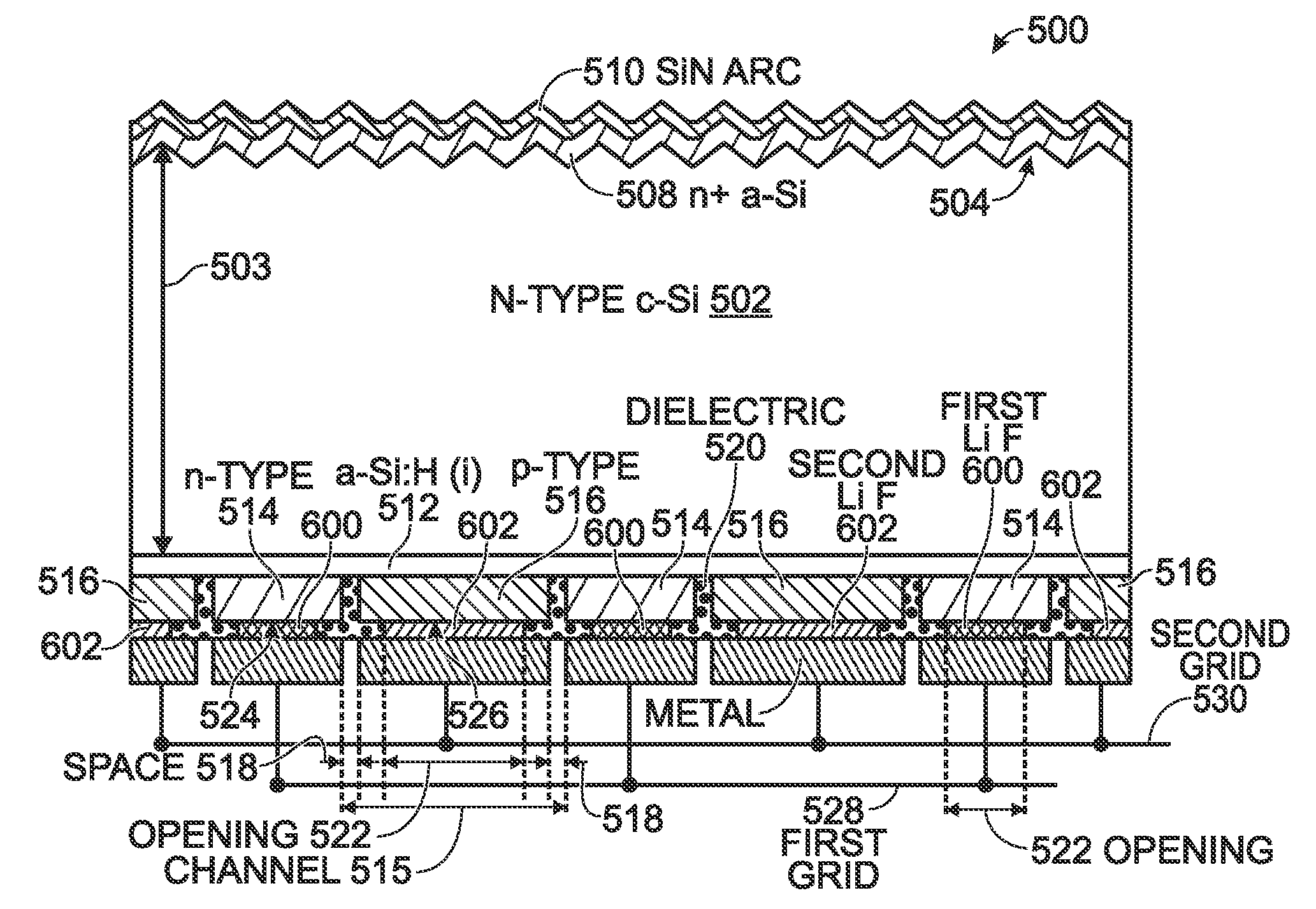
[0040]FIG. 5 is a partial cross-sectional view of an exemplary back contact solar cell with organic semiconductor heterojunctions. The solar cell 500 comprises a substrate 502 made from a first semiconductor of silicon lightly doped with a first dopant type having a first majority carrier and a first energy bandgap. The substrate 502 has a textured topside 504 and a backside 506. The substrate 502 first semiconductor is typically single-crystal silicon or multi-crystalline silicon. As shown in this example, the substrate 502 is n-type single-crystal silicon (c-Si). The substrate first semiconductor 502 has a thickness 503 in a range of 2 to 400 microns, with a first dopant density in a range of 5×10¹⁴ to 1×1016 cm−3.

[0041]A second semiconductor layer 508 overlies the first semiconductor substrate textured topside 504, made from hydrogenated amorphous silicon (a-Si:H) and doped with the first dopant. In this example, the first dopant is an n-type material such as arsenic (As) or phos...


PUM

PropertyMeasurementUnit
Thicknessaaaaaaaaaa
Carrier concentrationaaaaaaaaaa

Abstract

A back contact solar cell with organic semiconductor heterojunctions is provided. The substrate is made from silicon lightly doped with a first dopant type having a first majority carrier. A second semiconductor layer is formed overlying the texturized substrate topside, made from hydrogenated amorphous silicon (a-Si:H) and doped with the first dopant. An antireflective coating is formed overlying the second semiconductor layer. A third semiconductor layer is formed overlying the first semiconductor substrate backside, made from intrinsic a-Si:H. First and second majority carrier type organic semiconductor layers are formed overlying the third semiconductor layer in patterns. A dielectric organic semiconductor layer is formed overlying the first majority carrier type organic semiconductor layer and the second majority carrier type organic semiconductor layer, filling the spaces in the pattern. A first metal grid is connected to first organic semiconductor contact regions and a second metal grid is connected to the second organic semiconductor contact regions.

Description

RELATED APPLICATIONS[0001]This application is a Continuation-in-Part of a patent application entitled, SINGLE HETEROJUNCTION BACK CONTACT SOLAR CELL, invented by Jong-Jan Lee et al., Ser. No. 12 / 405,962, filed Mar. 17, 2009, Attorney Docket No. SLA2945, which is incorporated herein by reference.BACKGROUND OF THE INVENTION[0002]1. Field of the Invention[0003]This invention generally relates to solar cell fabrication and, more particularly, to an organic semiconductor heterojunction back contact solar cell and associated fabrication process.[0004]2. Description of the Related Art[0005]FIG. 1 is a partial cross-sectional view of a conventional silicon solar cell (prior art). The starting silicon wafer is usually lightly boron (p) doped. The emitter layer is formed by phosphorous (n) diffusion on the wafer front surface, and the back surface field is formed by either boron diffusion or by silicon-aluminum (Si—Al) eutectic formation. The front surface has antireflection coating (ARC) and...

Claims


Application Information

Patent Timeline
IPC IPC(8): H01L31/0352H01L51/46
CPCH01L31/022441H01L31/075B82Y30/00H01L51/0036H01L51/0037H01L51/0047B82Y10/00H01L51/4213H01L31/0747H01L31/1804Y02E10/548Y02E10/549Y02E10/547H01L51/4293Y02P70/50H10K85/113H10K85/1135H10K85/215H10K30/10H10K30/40
Inventor LEE, JONG-JANSCHUELE, PAUL J.
Owner SHARP LAB OF AMERICA INC SLA
Why Eureka
Try Eureka