MEMS-based getter microdevice

a micro-device and getter technology, applied in the field of micro-devices, can solve the problems of affecting the operation of the device housing, affecting the performance of the device, so as to prevent the degradation of the cmos circuitry or, achieve more precise pressure measurements

Active Publication Date: 2012-09-13
INSTITUT NATIONAL D'OPTIQUE
View PDF1 Cites 33 Cited by
  • Summary
  • Abstract
  • Description
  • Claims
  • Application Information

AI Technical Summary

Benefits of technology

[0015]The object of the present invention is a MEMS-based getter microdevice that can be fabricated according to a process flow compatible with those used for manufacturing typical MEMS devices and, in particular, VOx-based IR microbolometer array devices. The MEMS-based microdevice of the present invention allows localized heating of a thin-film getter material deposited on its surface without affecting its surroundings. The MEMS-based microdevice of the present invention can then be integrated with CMOS circuitry as well as with other MEMS microdevices. It can be reactivated several times during the lifetime of the package without impairing the performance of the microdevices or of the MEMS structures enclosed in the same microcavity. This is due to the fact that the getter takes the form of a locally-heated suspended structure that provides thermal insulation between the thin-film getter and the substrate. The MEMS getter microdevice can be coupled with pressure-sensing microdevices and temperature sensors, both fabricated using the same process flow and on a common substrate. The output signal from a pressure-sensing microdevice could serve to determine when the reactivation of the MEMS getter microdevice is needed. In turn, the temperature microsensors are to verify that the temperature around the MEMS getter microdevice does not raise beyond a predetermined maximum temperature, therefore preventing degradation of the CMOS circuitry or of the MEMS devices packaged in the microcavity. Note that the integration of temperature sensors with pressure microgauges also helps in obtaining more precise pressure measurements by allowing correction of the pressure readings to compensate for any temperature dependence in the operation of the pressure microgauges.

Problems solved by technology

For instance, devices made from III-V semiconductor materials are found to be particularly sensitive to outgassed gas species such as hydrogen, while moisture affects many semiconductor and MEMS devices.
Furthermore, changes in the ambient pressure in a microcavity can impair the operation of the devices housed therein.
Likewise, the presence of undesired gaseous species can degrade the device performance even if their partial pressures remain very low.
With the current trend in reducing the packaging size of IC's, MEMS, and optoelectronic / photonic microdevices, the control of the pressure, gas composition and gas concentration in the microcavities becomes a challenge, with the consequent increase in packaging costs and lower manufacturing yields.
Long outgassing runs performed at high temperature are normally required to reduce future outgassing from the various package components once the sealing step has been completed, thus reducing the throughput of the packaging process along with increasing costs.
The presence of moisture results in stiction problems in MEMS devices and to failures in semiconductor IC devices.
As vacuum / hermetic packages shrink, the electrically-activated getters, well known in the art, get too bulky to fit in these microcavities.
For example, alloys of zirconium have an activation temperature lying between 300° C. and 1000° C., while getter films made up of elemental zirconium or of titanium must be heated to 600-700° C. Unfortunately, these high activation temperatures can damage the semiconductor devices and MEMS microstructures integrated in the packages.
Furthermore, such high activation temperatures can damage the structural parts of a vacuum / hermetic package such as the hermetic joints, the antireflection coatings, and the die-attached materials.
In addition, heating the whole assembly to the activation temperature of the getter can generate a great deal of thermal stress to the assembly.
It is also well known that subjecting the whole package to such elevated temperatures can induce outgassing.
These solutions however, impact negatively on the complexity of the packages and on their costs.
These devices rely frequently on functionalized molecules that cannot withstand elevated temperatures.
The cavity volumes of the packages of current MEMS, semiconductor, electronics or photonics devices vary from a few nanoliters to thousands of microliters, therefore limiting seriously the room space available for insertion of conventional getters, as described above.
The layer 150 provides thermal insulation to protect the electronic devices 120, but this insulation may not be sufficient during activation of the getter 180.
As a consequence, attempts at reducing further the whole package size are seriously compromised.
However, a specific microfabrication process flow is necessary to implement the configuration depicted in FIG. 4, the process flow being not compatible with that of the MEMS devices to be integrated in the microcavity.
Unfortunately, the elevated temperatures (typically above 300° C.) required during performance of these bonding techniques can damage the devices (such as MEMS, photonic devices, or electronic devices) being packaged.
Those skilled in the art will appreciate the increased complexity of these packaging processes and their subsequent impacts on the manufacturing costs and throughput.

Method used


Image

  • MEMS-based getter microdevice
  • MEMS-based getter microdevice
  • MEMS-based getter microdevice

Examples


Embodiment Construction

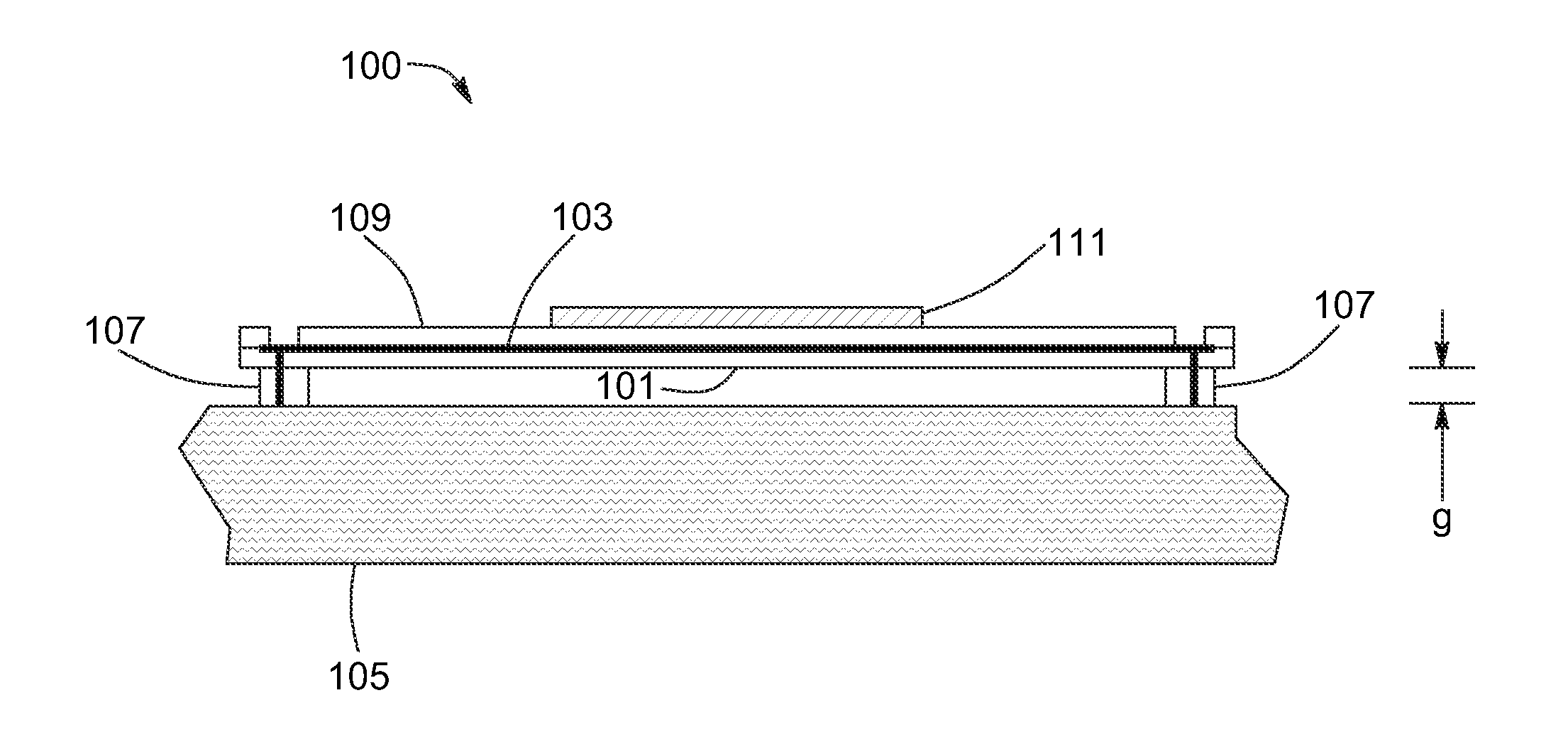
[0028]The accompanying drawings are not intended to be drawn to scale, and like reference numerals designate identical or corresponding parts throughout the views to be discussed in the following paragraphs. FIG. 5 illustrates a schematic cross-sectional side view of a preferred embodiment of a MEMS getter microdevice 100. The microdevice 100 includes a suspended structure (also referred to as a platform) 101 on which an electrically-resistive (resistor) element 103 has been patterned on its top surface. The suspended structure 101 is typically made up of a dielectric material such as but not limited to Si, SiO2, Si3N4 or silicon oxinitride. The structure 101 is supported by supporting legs 107 in such a way that a vertical gap g is formed above the substrate 105 on which the microdevice 100 is fabricated. The supporting legs 107 also provide thermal insulation of the suspended structure 101 and of the various layers deposited thereon. This means that the design of the supporting le...


PUM


Abstract

A MEMS (micro-electro-mechanical system) getter microdevice for controlling the ambient pressure inside the hermetic packages that enclose various types of MEMS, photonic, or optoelectronic devices. The getter microdevice revolves around a platform suspended at a height above a substrate, and which is supported by supporting legs having low thermal conductance. Layers are deposited on the platform, such layers including a properly patterned resistor element, a heat-spreading layer and, finally, a thin-film getter material. When an electrical current flows through it, the resistor element heats the thin-film getter material until it reaches its activation temperature. The getter material then absorbs the gas species that could be present in the hermetic package, such gas species possibly impairing the operation of the devices housed in the packages while reducing their lifetime. The weak thermal conductance between the platform and the substrate helps in preventing damages to the surrounding devices when the MEMS getter microdevice is heated at its activation temperature, and it reduces the electrical power required for reaching the activation temperature as well.

Description

FIELD OF THE INVENTION[0001]This invention relates to microdevices for controlling the ambient pressure inside the hermetic packages that enclose MEMS, photonic, and / or optoelectronic devices. More particularly, this invention relates to a MEMS microdevice integrated in a hermetic enclosure and consisting of an active thin-film getter used for controlling the gas composition and pressure therein.BACKGROUND OF THE INVENTION[0002]Several types of IC (integrated circuits), MEMS (micro-electro-mechanical systems) and optoelectronic / photonic devices need to be packaged in an inert or vacuum atmosphere to operate correctly. Outgassing, microleaks and diffusion are the most common mechanisms leading to a progressive increase of the pressure within vacuum / hermetic packages. These mechanisms also change the gas composition in the microcavity of hermetic packages. For instance, devices made from III-V semiconductor materials are found to be particularly sensitive to outgassed gas species such...

Claims


Application Information

Patent Timeline
Patent Type & Authority Applications(United States)
IPC IPC(8): H01L31/0216
CPCB81B7/0038
Inventor GARCIA-BLANCO, SONIAWILLIAMSON, FRASERVIENS, JEAN FRANCOIS
Owner INSTITUT NATIONAL D'OPTIQUE
Why Eureka
Try Eureka