Polishing method, polishing apparatus and polishing tool

a technology of polishing apparatus and surface, which is applied in the direction of lapping machines, semiconductor/solid-state device testing/measurement, instruments, etc., can solve the problems of difficult to planarize the surface of a single substrate made of a compound semiconductor, and achieve high polishing rate, and high level of flatness

Active Publication Date: 2012-09-27
OSAKA UNIV +1
View PDF1 Cites 23 Cited by
  • Summary
  • Abstract
  • Description
  • Claims
  • Application Information

AI Technical Summary

Benefits of technology

[0065]A polishing method and a polishing apparatus according to the present invention are capable of finishing a surface of a substrate, which is made of a compound semiconductor containing an element such as Ga or the like, to a high level of flatness. By combining the finishing process with a polishing process involving the application of light and / or the application of a bias potential, i.e., by polishing the surface of the substrate at a high polishing rate with the application of light and / or the application of a bias potential, and subsequently finishing the surface of the substrate to a high level of flatness, the time required to polish the surface of the substrate, which is made of a compound semiconductor containing an element such as Ga or the like, can greatly be reduced.
[0066]According to another polishing method and the polishing apparatus of the present invention, even if the substrate is a bare substrate, for example, which is made of only a semiconductor with no film on its surface, a damage level of the surface of the substrate can be measured by a photocurrent-type damage level measuring system, a photoluminescence-light-type damage level measuring system, or a Raman-light-type damage level measuring system while at the same time the surface of the substrate is being polished, and the progress of the polishing process can be monitored.
[0067]According to a polishing toll of the present invention, since the support platen and the catalyst pad are separate from each other and the catalyst pad has a high level of surface flatness and does not tend to produce burrs, scratches, etc., the polishing tool is capable of producing a flat polished surface free of burrs, scratches, etc. The catalyst can be replaced with a new one by replacing the catalyst pad, while allowing the support platen to be reused. Accordingly, the polishing tool is inexpensive and highly durable.
[0068]Further, since the elastic base of elastic material is elastically deformable along the surface (polished surface) of the substrate, even if the elastic base has surface irregularities, they are prevented from being transferred to the surface of the substrate. Inasmuch as the intermediate film made of carbon or chromium is interposed between the elastic base and the electrically conductive member for increasing adhesion therebetween, the adhesion between the elastic base and the electrically conductive member is increased by the intermediate film, so that the electrically conductive member is less liable to be peeled off from the elastic base.

Problems solved by technology

However, it is generally difficult to planarize a surface of a single substrate made of a compound semiconductor containing an element Ga, for example, to a sufficiently highly accurate surface roughness within a practical given period of time.

Method used


Image

  • Polishing method, polishing apparatus and polishing tool
  • Polishing method, polishing apparatus and polishing tool
  • Polishing method, polishing apparatus and polishing tool

Examples


example 1

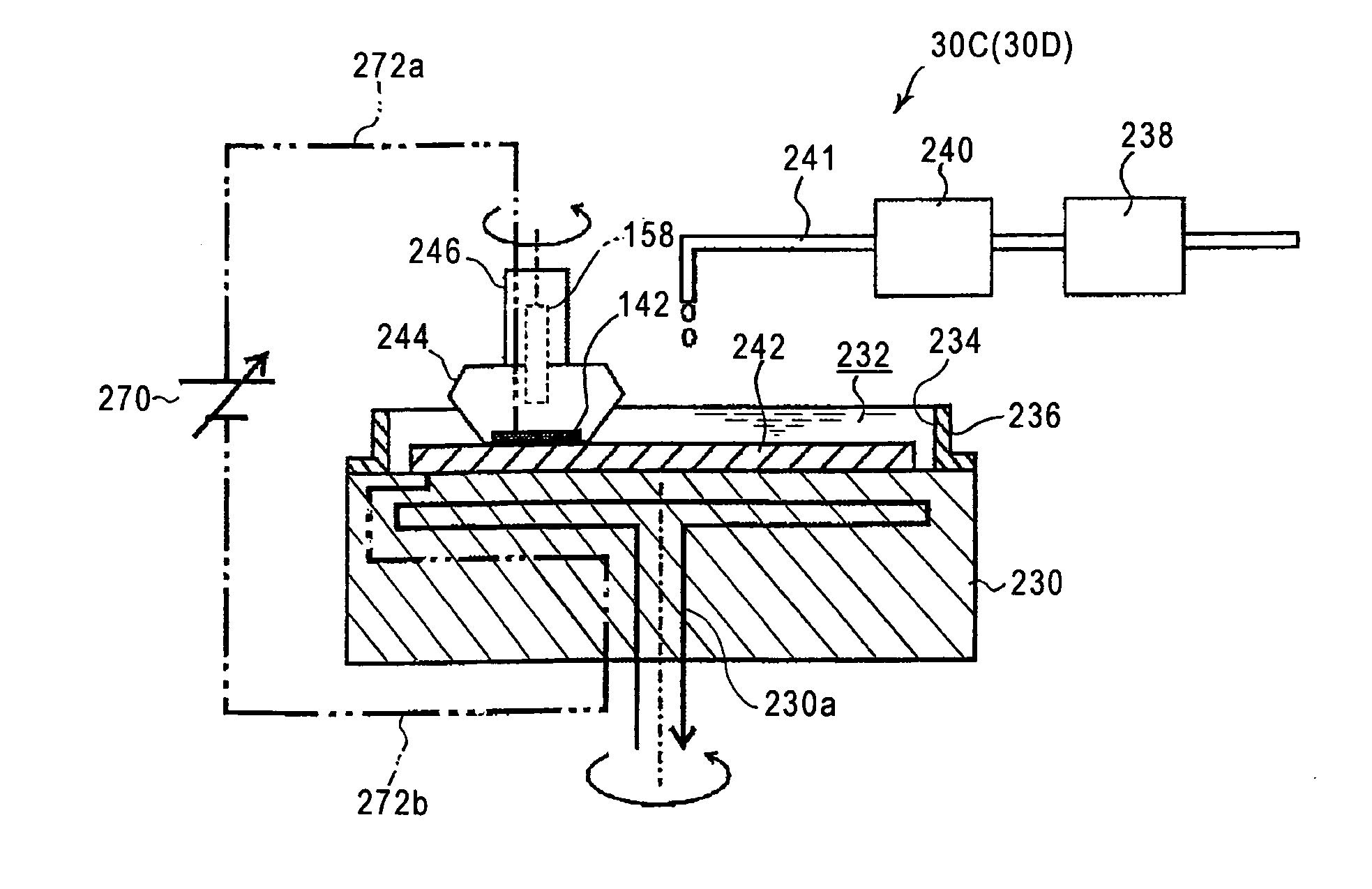
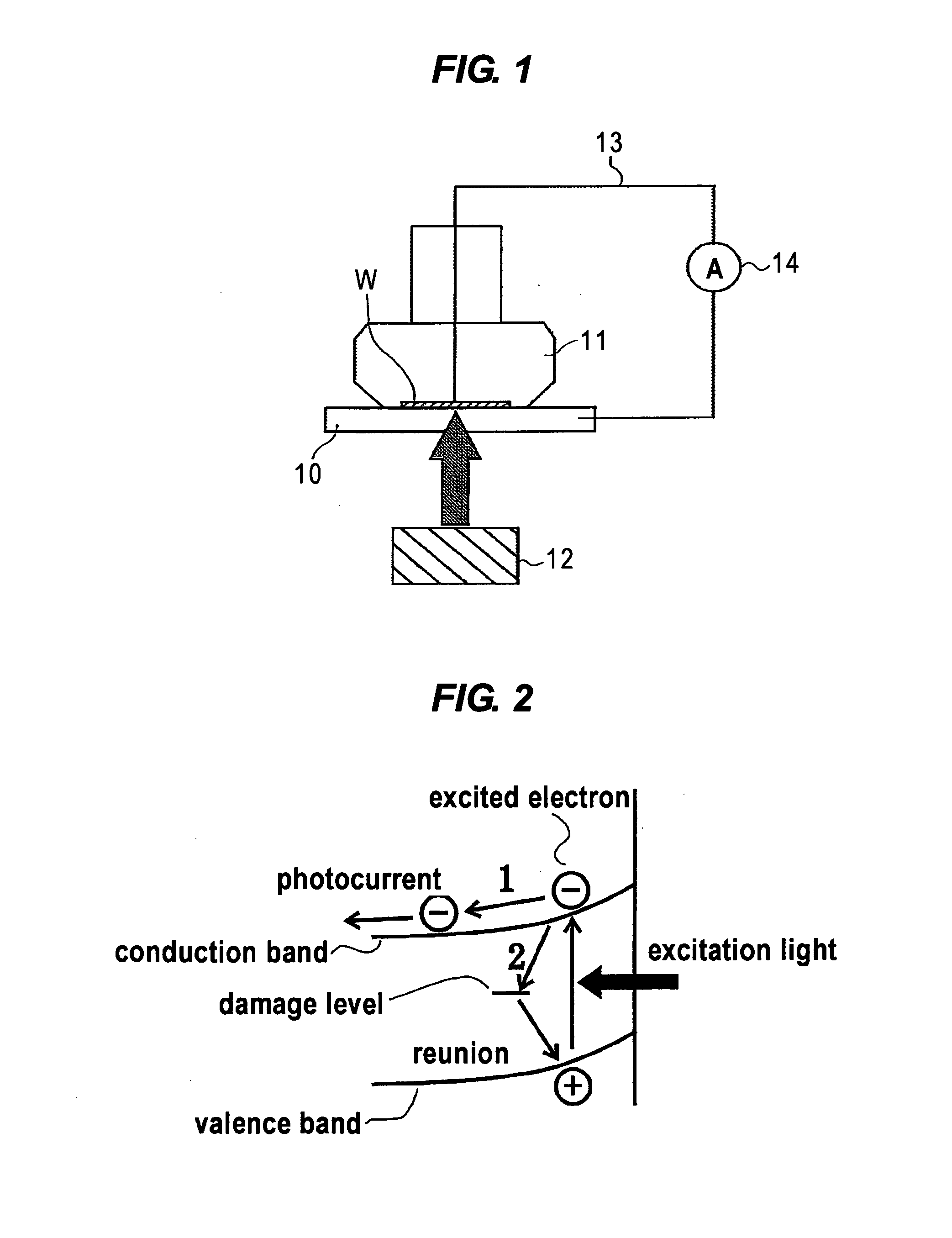
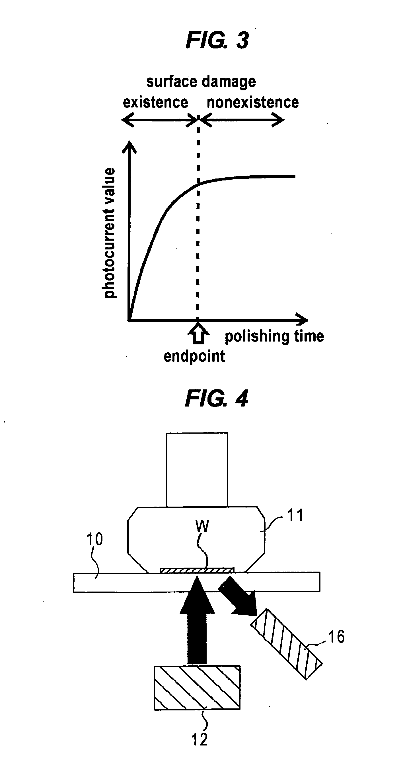
[0182]A GaN substrate was prepared by polishing a substrate surface in the first stage by applying excitation light and a voltage and then polishing the substrate surface in the second stage by applying only excitation light. The surface of the GaN substrate was polished (finished) in the third stage by the polishing apparatus shown in FIG. 14. In the polishing apparatus shown in FIG. 14, the electrically conductive member 264 was made of platinum, and water 232 with its pH adjusted to 5.5 by dissolving CO2 in pure water with the gas dissolver 238 was poured into the container 234 provided by the dam member 236. The surface of the GaN substrate was polished for 3 hours by rotating the turntable 230 at a rotational speed of 10 rpm and holding the substrate surface and the electrically conductive member (platinum) 264 in contact with each other under a contact pressure (pressing force) of 0.4 kgf / cm2.

[0183]An atomic force microscope (AFM) image of the GaN substrate surface after it is...

example 2

[0186]A GaN substrate surface was polished under the same conditions as Example 1 except that a bonded substrate (epitaxial substrate) with GaN mounted on a surface of a sapphire substrate was used instead of the GaN substrate made of only GaN.

[0187]An atomic force microscope (AFM) image of the substrate surface after it is polished is shown in FIG. 25A, the relationship between distances and heights on the substrate surface is shown in FIG. 25B. Any etch pits depending on crystal defects are not observed from FIG. 25A, and a clear terrace-step structure is observed from FIG. 25B, indicating that the substrate surface was polished in an atomic level to a flat damageless finish.

[0188]In this Example 2, the bonded substrate with GaN mounted on the surface of the sapphire substrate. It is also possible to polish a bonded substrate with GaN mounted on a surface of a SiC substrate, a bonded substrate with GaN mounted on a surface of a Si substrate, or a bonded substrate with GaN mounted ...


PUM

PropertyMeasurementUnit
band gapaaaaaaaaaa
pHaaaaaaaaaa
to-valley)aaaaaaaaaa

Abstract

A polishing method and a polishing apparatus particularly suitable for finishing a surface of a substrate of a compound semiconductor containing an element such as Ga or the like to a desired level of flatness, so that a surface of a substrate of a compound semiconductor containing an element of Ga can be flattened with high surface accuracy within a practical processing time. In the presence of water (232) such as weak acid water, water with air dissolved therein, or electrolytic ion water, a surface of a substrate (142) made of a compound semiconductor containing either one of Ga, Al, and In and the surface of a polishing pad (242) having an electrically conductive member (264) in an area of the surface which is held in contact with the substrate (142) are relatively moved while being held in contact with each other, thereby polishing the surface of the substrate (142).

Description

TECHNICAL FIELD[0001]The present invention relates to a polishing method and a polishing apparatus, and more particularly to a polishing method and a polishing apparatus for performing the planarization polishing of a surface (surface to be processed) of a substrate such as a single substrate made of a compound semiconductor containing an element such as Ga, Al, In, or the like, or a bonded substrate (epitaxial substrate) on which a compound semiconductor containing an element such as Ga, Al, In, or the like is mounted. The present invention is also related to a polishing method and a polishing apparatus, such as a catalyst-referred chemical processing system, for performing the planarization polishing of a surface (surface to be processed) of a substrate while monitoring the progress of a polishing process in order to determine the timing of an endpoint of the polishing process. (e. g., stoppage of polishing process or change of polishing conditions). Furthermore, the present inven...

Claims


Application Information

Patent Timeline
Patent Type & Authority Applications(United States)
IPC IPC(8): H01L21/66H01L21/306B24B37/04
CPCB24B37/0053B24B37/042B24B37/10H01L21/32125B24B49/12H01L21/02024B24B37/30
Inventor SANO, YASUHISAYAMAUCHI, KAZUTOMURATA, JUNJIOKAMOTO, TAKESHISADAKUNI, SHUNYAGI, KEITA
Owner OSAKA UNIV
Why Eureka
Try Eureka