Programmable logic device

a logic device and programmable logic technology, applied in the field can solve the problems of low power consumption of programmable logic devices, high writing voltage of eeproms, and limitation of the number of reads of ferams, etc., to achieve high integration, low power consumption, and short start-up time

Inactive Publication Date: 2012-11-01
SEMICON ENERGY LAB CO LTD
View PDF2 Cites 23 Cited by
  • Summary
  • Abstract
  • Description
  • Claims
  • Application Information

AI Technical Summary

Benefits of technology

[0021]According to an embodiment of the present invention, a configuration memory is formed using a non-volatile memory element including a transistor whose channel region is in an oxide semiconductor film and an arithmetic circuit; therefore, data can be held in the configuration memory even when supply of power is stopped. As a result, a programmable logic device can have short start-up time and operate with low power. The memory element included in the configuration memory can be highly integrated because the arithmetic circuit and the transistor whose channel region is in an oxide semiconductor film can be stacked.

Problems solved by technology

However, writing voltage of an EEPROM is high.
In the case of using an EEPROM as the configuration memory, a step-up circuit is needed for writing of configuration data, that is a disadvantage in higher integration and lower power consumption of the programmable logic device.
A FeRAM has limitation on the number of reads and thus is not appropriate as the configuration memory.

Method used


Image

  • Programmable logic device
  • Programmable logic device
  • Programmable logic device

Examples


embodiment 1

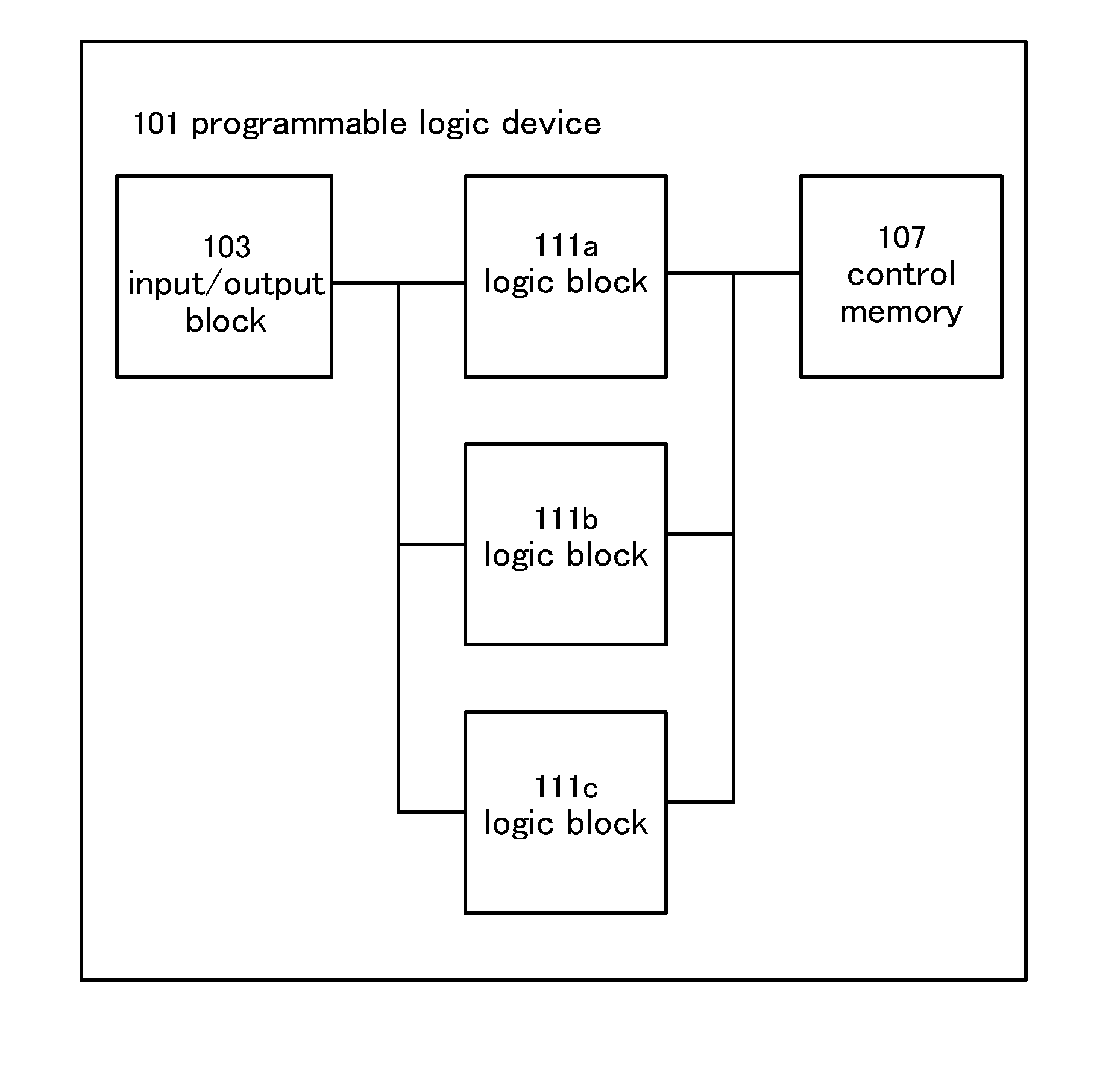
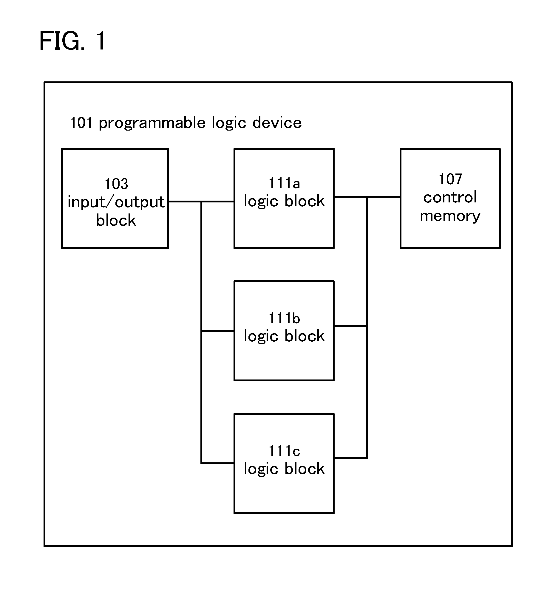
[0058]One mode of a programmable logic device is described with reference to FIG. 1, FIG. 2, FIG. 3, FIGS. 4A to 4C, FIG. 5, FIG. 6, and FIG. 7.

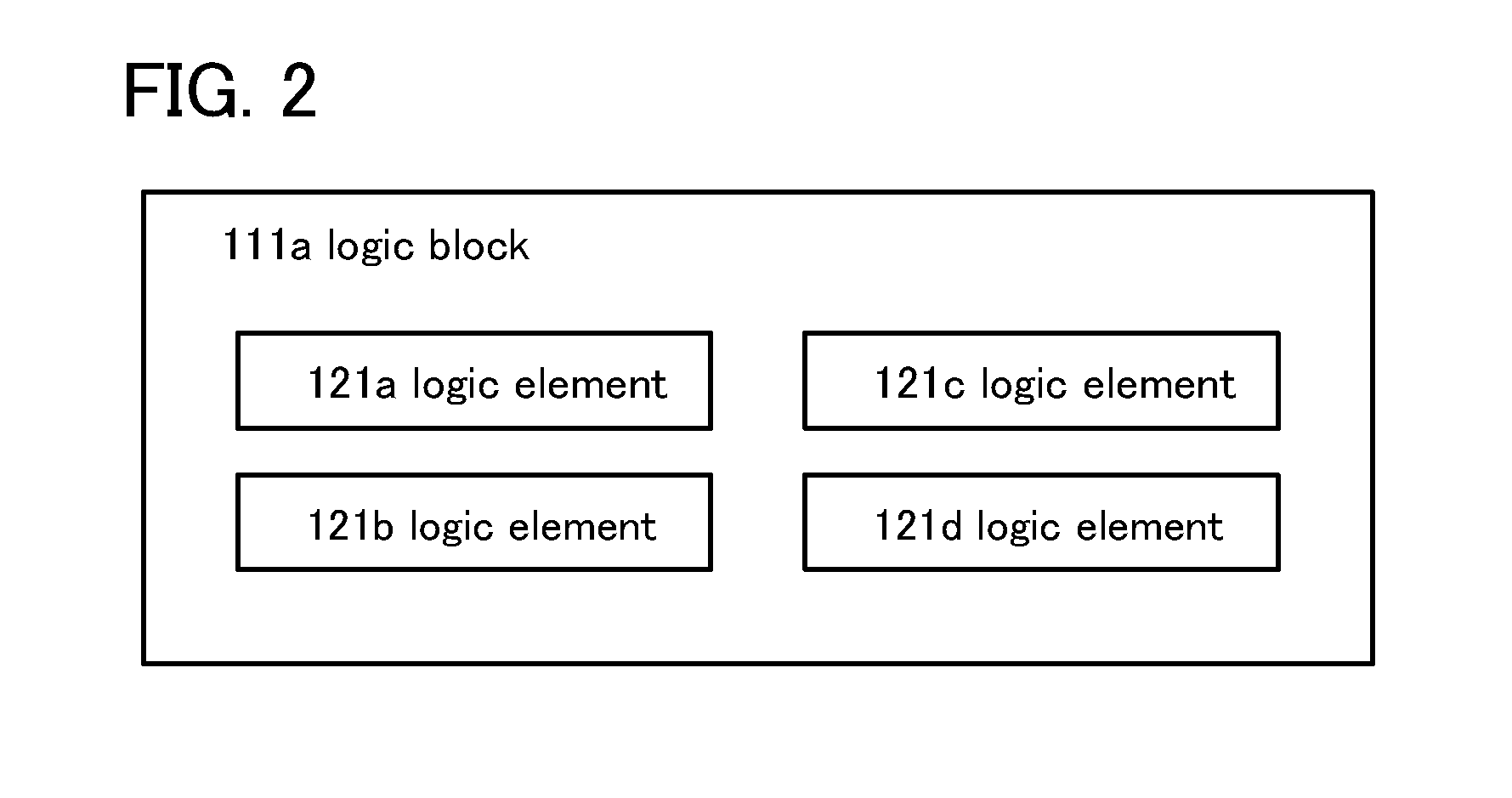
[0059]FIG. 1 is a block diagram of one mode of a programmable logic device 101. The programmable logic device 101 includes an input / output block 103; a plurality of logic blocks 111a, 111b, and 111c, which have various functions; wirings; and a control memory 107; which are provided on the periphery of the programmable logic device 101. The connection of the wirings can be changed by a switch or the like.

[0060]The input / output block 103 controls transmission and reception of signals between the programmable logic device and the outside thereof. For typical example, the input / output block 103 sets a signal input from or output to an external terminal of the programmable logic device.

[0061]The control memory 107 holds data (configuration data) to be written to configuration memories included in the logic blocks 111a to 111c. The control memory...

embodiment 2

[0128]In this embodiment, a method for manufacturing the programmable logic device described in Embodiment 1 is described with reference to FIG. 7, FIGS. 8A to 8D, FIGS. 9A to 9C, FIGS. 10A to 10C, and FIGS. 11A and 11B. Here, the memory element 141 which has the transistor 161 including an oxide semiconductor film and a buffer functioning as the arithmetic circuit 163 as illustrated in a circuit diagram in FIG. 7 is described as a memory element. Specifically, as a method for manufacturing the programmable logic device, a method for manufacturing the transistor 161 including an oxide semiconductor film and the first n-channel transistor 163a and the first p-channel transistor 163b which form the buffer is described. Note that in FIGS. 8A to 8D, FIGS. 9A to 9C, FIGS. 10A to 10C, and FIGS. 11A and 11B, cross-sectional views taken along a line A-B each correspond to a cross-sectional view of a region where the transistor 161 including an oxide semiconductor film, the first n-channel t...

embodiment 3

[0257]In this embodiment, a method for forming the oxide semiconductor film 229 described in Embodiment 2 using a CAAC-OS will be described.

[0258]The first method for forming the oxide semiconductor film 229 using a CAAC-OS will be described below.

[0259]In the case where a sputtering method is employed in the method for forming an oxide semiconductor film to be the oxide semiconductor film 227 described in FIG. 9B in Embodiment 2 in forming the oxide semiconductor film 229 using a CAAC-OS, the substrate temperature is set to be higher than or equal to 150° C. and lower than or equal to 450° C., preferably higher than or equal to 200° C. and lower than or equal to 350° C., so that entry of water (including hydrogen) to the oxide semiconductor film can be prevented and a CAAC-OS including crystals can be formed.

[0260]The oxide semiconductor film is heated after formation using a CAAC-OS by the above-described method releases further hydrogen from the oxide semiconductor film 227, can ...


PUM


Abstract

An object of the present invention is to provide a programmable logic device which has short start-up time after supply of power is stopped, is highly integrated, and operates with low power. In a programmable logic device including an input/output block, a plurality of logic blocks each including a logic element, and a wiring connecting the plurality of logic blocks, the logic element has a configuration memory for holding configuration data and a look-up table including a selection circuit. The configuration memory includes a plurality of memory elements each of which includes a transistor whose channel region is in an oxide semiconductor film and an arithmetic circuit provided between the transistor and the selection circuit. Configuration data is selectively changed and output by the selection circuit in accordance with an input signal.

Description

BACKGROUND OF THE INVENTION[0001]1. Field of the Invention[0002]The present invention relates to a programmable logic device. The present invention further relates to a semiconductor device using the programmable logic device, and an electronic device using the semiconductor device.[0003]2. Description of the Related Art[0004]Programmable logic devices show flexibility in a reduction in development period and a change in design specification as compared to conventional application specific integrated circuits (ASIC) and gate arrays, which is advantageous. Therefore, a semiconductor device including the programmable logic device has been developed actively.[0005]The programmable logic device includes, for example, a plurality of logic blocks each including a plurality of logic elements, wirings connecting the a plurality of logic blocks, and an input / output block. When the functions of the logic elements are changed, the function of the programmable logic device can be changed.[0006]...

Claims


Application Information

Patent Timeline
Patent Type & Authority Applications(United States)
IPC IPC(8): H03K19/177H03K19/0948H03K19/094
CPCH03K19/17728H01L27/11803H03K19/17772H03K19/1776
Inventor NISHIJIMA, TATSUJI
Owner SEMICON ENERGY LAB CO LTD
Why Eureka
Try Eureka