Method for manufacturing semiconductor device, substrate processing apparatus, and semiconductor device

Inactive Publication Date: 2012-11-08
KOKUSA ELECTRIC CO LTD
View PDF16 Cites 16 Cited by
  • Summary
  • Abstract
  • Description
  • Claims
  • Application Information

AI Technical Summary

Benefits of technology

[0022]According to the present invention, different modification treatments such as sufficiently oxidizing

Problems solved by technology

Reversely, in a case that an oxidizing agent having a weak oxidizing power is used for preventing oxidation of the lower electrode, oxidation of the High-k film becomes insufficient, and the dielectric constant of the High-k film can't be sufficiently increased, thus causing the reduction of the capacitor capacitance to be reduced in some cases.
Further, all raw materials that constitute the High-k film can't be completely oxidized in some cases, due to an insufficient oxidizing power of the oxidizing agent used for forming the High-k film, and an incomplete film forming condition, etc.
In such a case, oxygen in the High-k film is deficient or carbon (C) is remained in the High-k film, thus involving a problem that defect is generated in the High-k film.
Then, current flows with such a defect as a route, thus increasing a leak current of the capacitor, or deteriorating the capacitor in some cases.
Further, oxidation of the insulating film becomes insufficient in some cases, by suppressing the oxidation of the metal film.
Namely, it is difficult to simultaneously perform different modification treatments such as oxidizing the insulating film, and such as suppressing oxidation of the metal film.

Method used


Image

  • Method for manufacturing semiconductor device, substrate processing apparatus, and semiconductor device
  • Method for manufacturing semiconductor device, substrate processing apparatus, and semiconductor device
  • Method for manufacturing semiconductor device, substrate processing apparatus, and semiconductor device

Examples


first embodiment

of the Present Invention

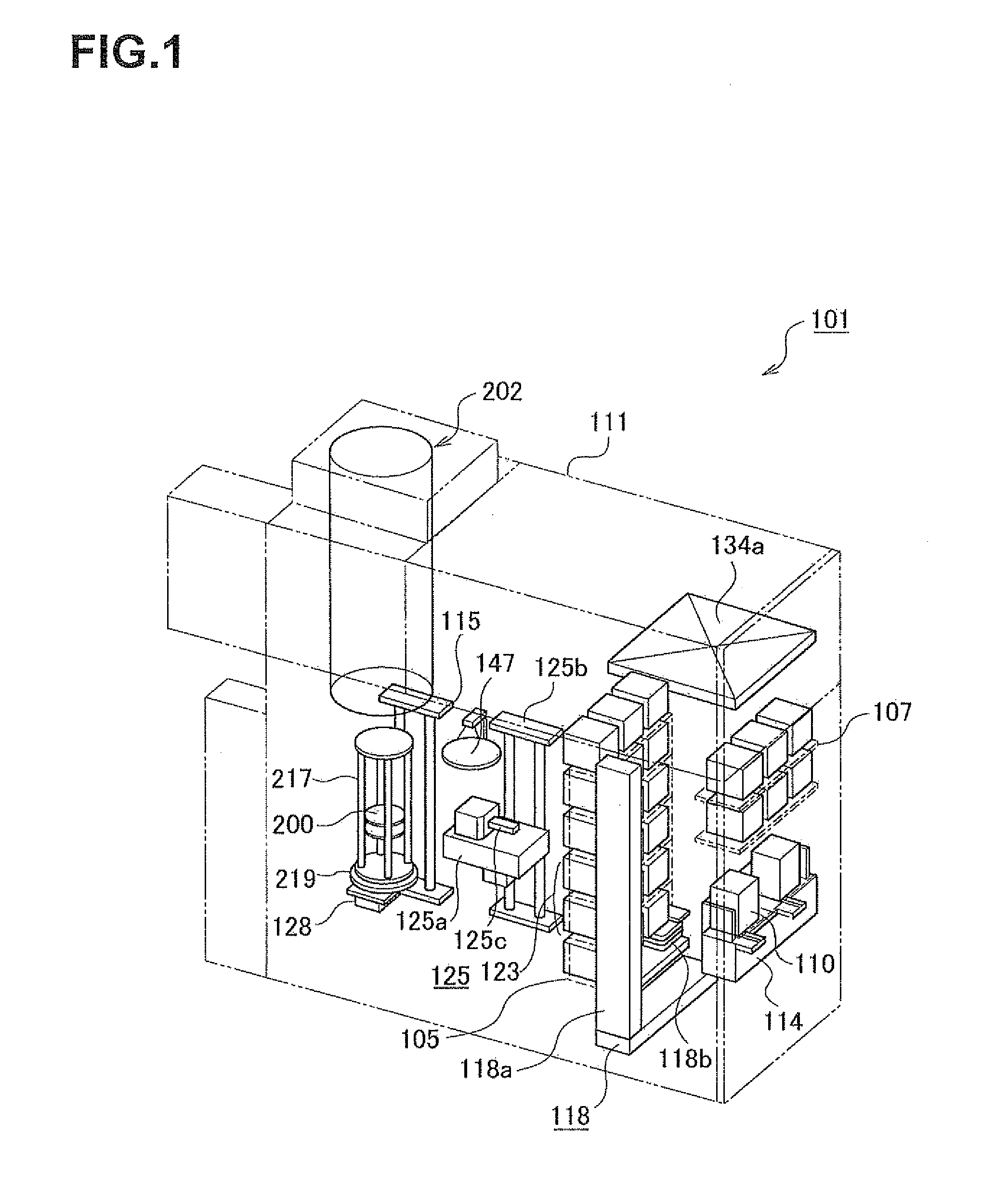
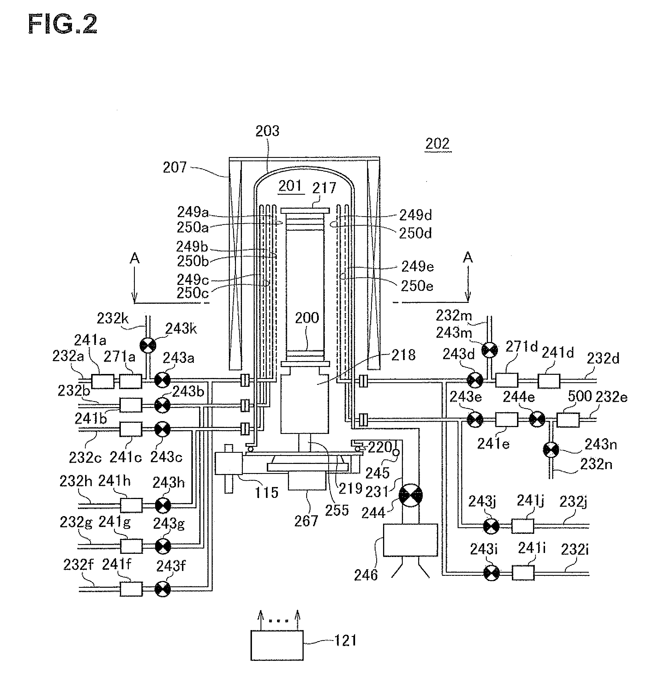
[0045]First, a constitutional example of a substrate processing apparatus according to a first embodiment of the present invention will be described, using FIG. 1 to FIG. 3. FIG. 1 is a perspective transparent view of a substrate processing apparatus 101 according to this embodiment. FIG. 2 is a side cross-sectional view of a treating furnace 202 according to this embodiment.

[0046]FIG. 3 is an upper side cross-sectional view of the treating furnace 202 according to this embodiment, showing a treating furnace 202 portion taken along the line A-A of FIG. 2.

[0047](Structure of the Substrate Processing Apparatus)

[0048]As shown in FIG. 1, the substrate processing apparatus 101 according to this embodiment comprises a housing 111. In order to carry each wafer (substrate) 200 made of silicon, etc., to inside / outside the housing 111, a cassette 110, being a wafer carrying device (substrate housing vessel) for housing a plurality of wafers 200, is used. A cassette sta...

example

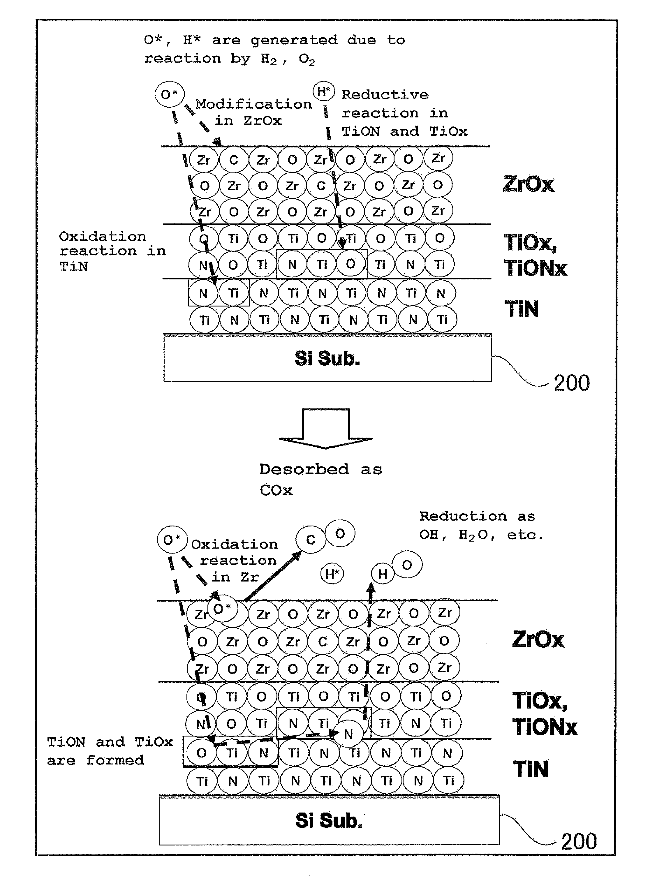
[0167]In this example, the TiN film and the ZrO film are laminated on the wafer by the same technique as the technique of the aforementioned embodiment, and thereafter different modification treatments are simultaneously performed to the ZrO film and the TiN film using O2 gas and H2 gas. Then, a composition of the TiN film after modification treatment (reduction treatment) was measured by X-ray Photoelectron Spectroscopy (abbreviated as XPS). Further, EOT (an equivalent oxide film thickness) and leak current density of the ZrO film after modification treatment (oxidation treatment) were respectively measured. Note that a wafer temperature during the modification treatment was set to 45 to 500° C., and a gas supply time (irradiation time) during the modification treatment was set to 5 to 60 minutes. A voltage applied to the ZrO film during measurement of the EOT and the lead current density was set to −1.0V.

[0168]Further, as a reference example, the TiN film and the ZrO film were for...

second embodiment

of the Present Invention

[0177]This embodiment is a modified example of the first embodiment. In this embodiment, the oxygen-containing gas and the hydrogen-containing gas are alternately supplied to the wafer 200 on which the TiN film and the ZrO film are exposed or laminated, and the oxidation treatment of the ZrO film as a modification treatment shown in the first embodiment, and an individual modification treatment such as a reduction treatment of the TiN film, are sequentially executed. Thereafter, as a final step of the modification treatment, the oxygen-containing gas and the hydrogen-containing gas are simultaneously supplied to the wafer 200, to thereby simultaneously execute different modification treatments (oxidation of the ZrO film and reduction of the TiN film).

[0178]FIG. 8 is a timing chart of supplying gas in the substrate processing step according to this embodiment, and FIG. 9 is a timing chart of supplying gas in the modification treatment according to this embodim...


PUM

PropertyMeasurementUnit
Lengthaaaaaaaaaa

Abstract

There is provided a method for manufacturing a semiconductor device, comprising simultaneously or alternately exposing a substrate, which has two or more kinds of thin films having different elemental components laminated or exposed; and performing different modification treatments to the thin films respectively.

Description

TECHNICAL FIELD[0001]The present invention relates to a method for manufacturing a semiconductor device having a step of processing a substrate, a substrate processing apparatus used for executing this method, and a semiconductor device manufactured by this method or this apparatus.DESCRIPTION OF RELATED ART[0002]CVD (Chemical Vapor Deposition) method can be given as one of the techniques of forming a prescribed film on a substrate. The CVD method is a method of forming a film on the substrate, with an element contained in a raw material molecule as a constituent element, by utilizing a reaction of two or more kinds of raw materials in a gas phase or on a surface of the substrate. Further, ALD (Atomic Layer Deposition) method can be given as one of the CVD methods. Two kinds of raw materials used for film formation, are supplied to the substrate alternately one by one, under a certain film forming condition (temperature and time, etc.), which is then adsorbed on the substrate by an ...

Claims


Application Information

Patent Timeline
IPC IPC(8): C23C16/52H01L29/02H01L21/02
CPCC23C16/405C23C16/45527C23C16/45561C23C16/45563C23C16/56H01L21/02189C23C16/45578H01L21/02337H01L21/02356H01L28/40H01L28/60C23C16/34H01L21/0228
Inventor SAITO, TATSUYUKIYUASA, KAZUHIROHIROSE, YOSHIROTAKEBAYASHI, YUJISASAJIMA, RYOTAYAMAMOTO, KATSUHIKOYAMAZAKI, HIROHISAKOGURA, SHINTAROHAMAMURA, HIROTAKA
Owner KOKUSA ELECTRIC CO LTD
Why Eureka
Try Eureka