

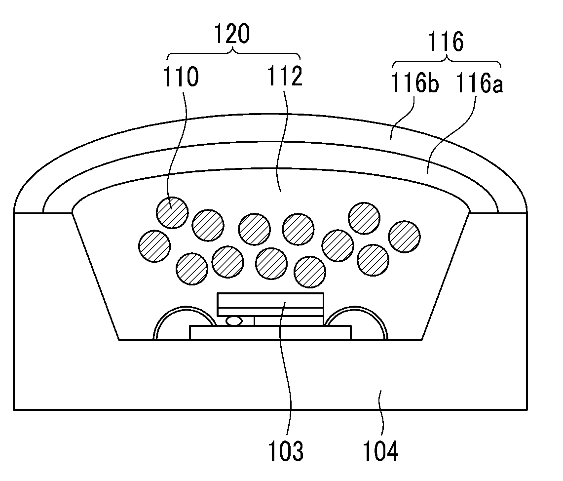
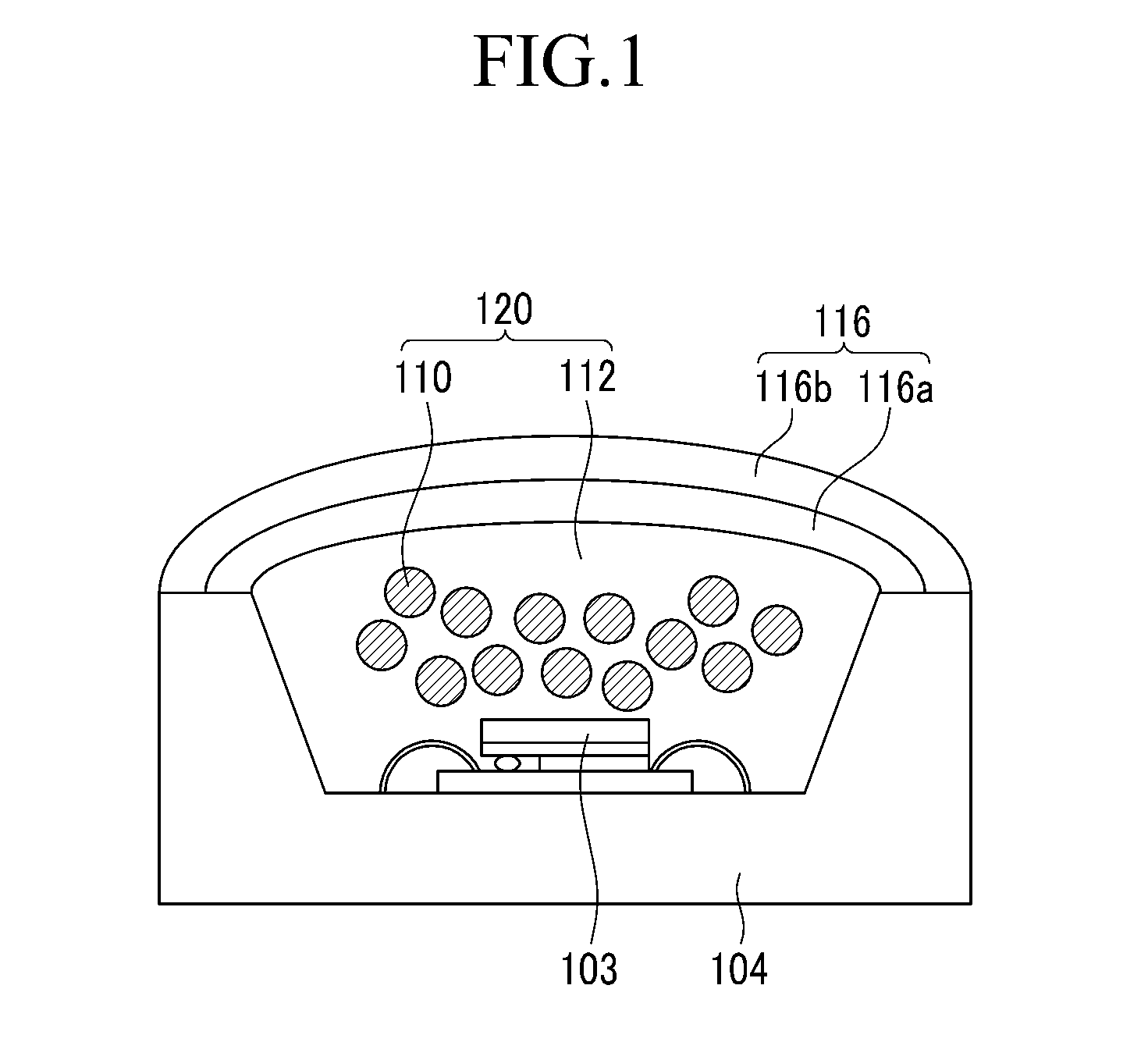
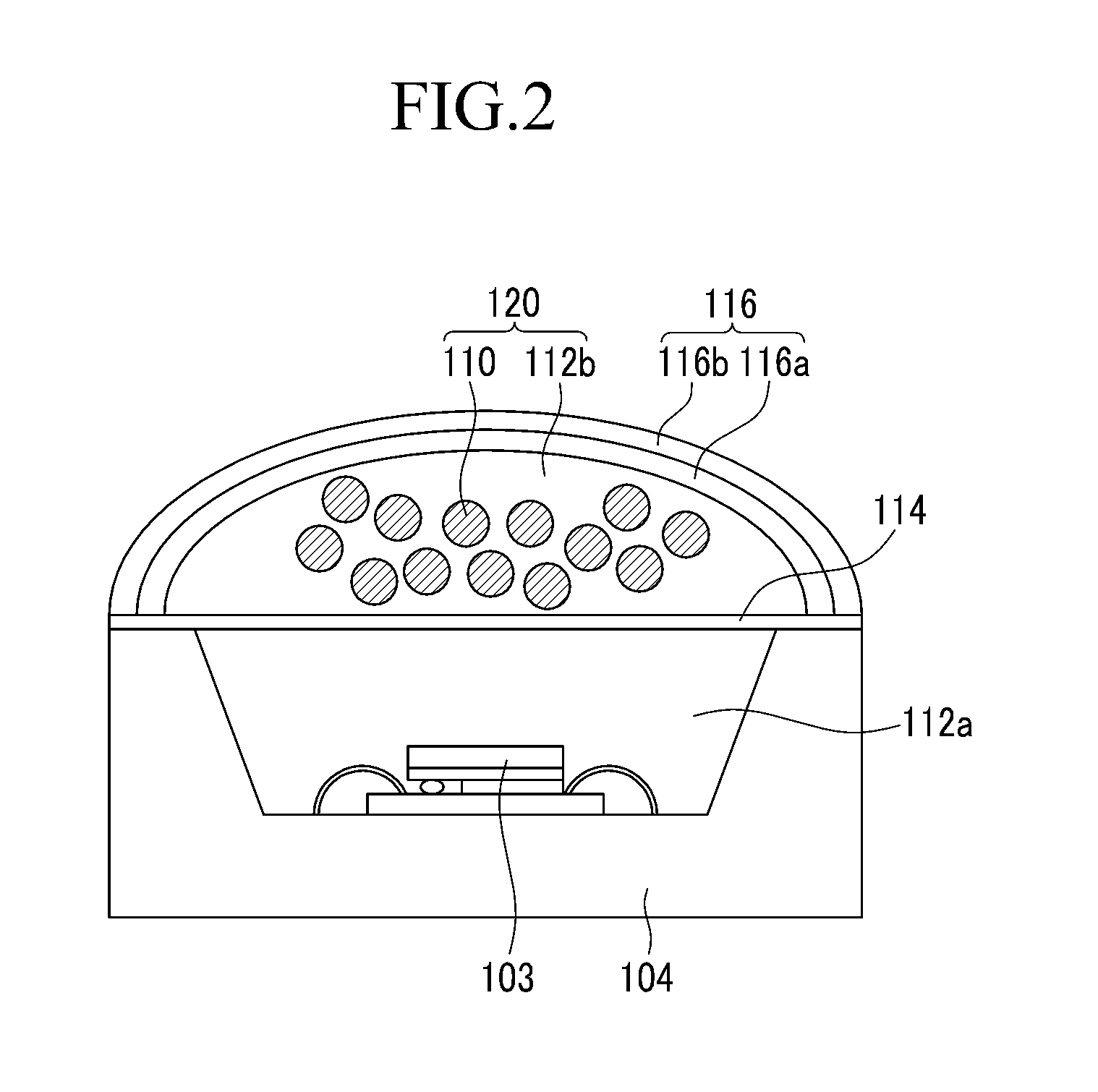
Optoelectronic device and stacking structure
a technology of optoelectronic devices and stacking structures, which is applied in the direction of discharge tubes/lamp details, discharge tubes luminescent screens, discharge tubes/lamp details, etc., can solve the problems that silicon polymer may not sufficiently protect the semiconductor nanocrystal, and achieve excellent oxygen or moisture barrier properties, improve the efficiency or the life-span of an optoelectronic device
- Summary
- Abstract
- Description
- Claims
- Application Information
AI Technical Summary
Benefits of technology
Problems solved by technology
Method used
Image

Examples
preparation example 1
Synthesis of a nanocrystal
[0160]About 16 grams (“g”) of trioctylamine (“TOA”), about 0.3 g of octadecyl phosphonic acid, and 0.4 millimoles (“mmol”) of cadmium oxide are simultaneously introduced into a 125 milliliter (“ml”) flask mounted with a reflux condenser under vacuum while undergoing agitation, and heated to about 120° C. Then, after the temperature reaches about 120° C., nitrogen is flowed therein and the reaction temperature is increased to about 300° C.
[0161]Separately, selenium (“Se”) powder is dissolved in trioctylphosphine (“TOP”) to provide a 2 M Se-TOP complex solution. About 2 ml of 2 M Se-TOP complex solution is quickly injected into the reaction mixture that is agitated at about 300° C. and reacted for about 2 minutes.
[0162]After completing the reaction, the temperature of the reaction mixture is cooled as quickly as possible to room temperature, and a non-solvent of ethanol is added and centrifugation is performed. The supernatant of the solution excluding the ce...
example 1
Fabrication of Light Emitting Diode (LED) Device
[0169]OE6630A, and pentaerythritol tetrakis(3-mercaptopropionate) are mixed in a weight ratio of about 2:1 to provide a solution that is mixed with oxy-phenyl-acetic acid 2-[2-oxo-2-phenyl-acetoxy-ethoxy]-ethyl ester at about 1 wt %. The solution is coated on the cured silicone resin of the light emitting diode device according to Comparative Example 1 and UV cured for about 20 minutes to provide a first polymer layer.
[0170]Pentaerythritol tetrakis(3-mercaptopropionate) and 1,3,5-triallyl-1,3,5-triazine-2,4,6-trione are mixed at a mole ratio of about 3:4 and mixed with about 1 wt % of oxy-phenyl-acetic acid 2-[2-oxo-2-phenyl-acetoxy-ethoxy]-ethyl ester and coated on the first polymer layer. The contact angle of this second polymer layer coated on the first polymer layer is about 12 degrees. The coated mixture is UV cured for about 10 minutes to provide a light emitting diode device formed with the polymer film
example 2
Fabrication of Light Emitting Diode (LED) Device
[0171]A light emitting diode device formed with a polymer film is fabricated in accordance with the same procedure as in Example 1, except that the siloxane-containing oligomer of the first polymer layer is OE6630B. The contact angle of the second polymer layer coated on the first polymer layer is about 19 degrees.
PUM
 Abstract
Description
Claims
Application Information