Switching device having a non-linear element

a non-linear element and switching memory technology, applied in the direction of semiconductor devices, electrical equipment, code conversion, etc., can solve the problems of increased power dissipation, non-scaling of sub-threshold slopes, and preventing proper device operation, so as to achieve high switching speed and low leakage current characteristics , the effect of high density

Active Publication Date: 2012-12-06
CROSSBAR INC
View PDF4 Cites 60 Cited by
  • Summary
  • Abstract
  • Description
  • Claims
  • Application Information

AI Technical Summary

Benefits of technology

[0010]The present invention has a number of advantages over conventional techniques. For example, embodiments of the present invention allow for a high density non-volatile memory characterized by high switching speed, l

Problems solved by technology

However, as field effect transistors (FET) approach sizes less than 100 nm, problems such as short channel effect start to prevent proper device operation.
Moreover, such sub 100 nm device size can lead to sub-threshold slope non-scaling and increased power dissipation.
These devices often require new materials and device structures to couple with silicon based devices to form a memory cell, which lack one or more key attributes.
For example, Fe-RAM and MRAM devices have fast switching characteristics and good programming endurance, but their fabrication is not CMOS compatible and size is usually large.
Switching for a PCRAM device uses Joules heating, which inherently has high power consumption.
Organic RAM or ORAM is incompatible with large volume silicon ba

Method used


Image

  • Switching device having a non-linear element
  • Switching device having a non-linear element
  • Switching device having a non-linear element

Examples


Embodiment Construction

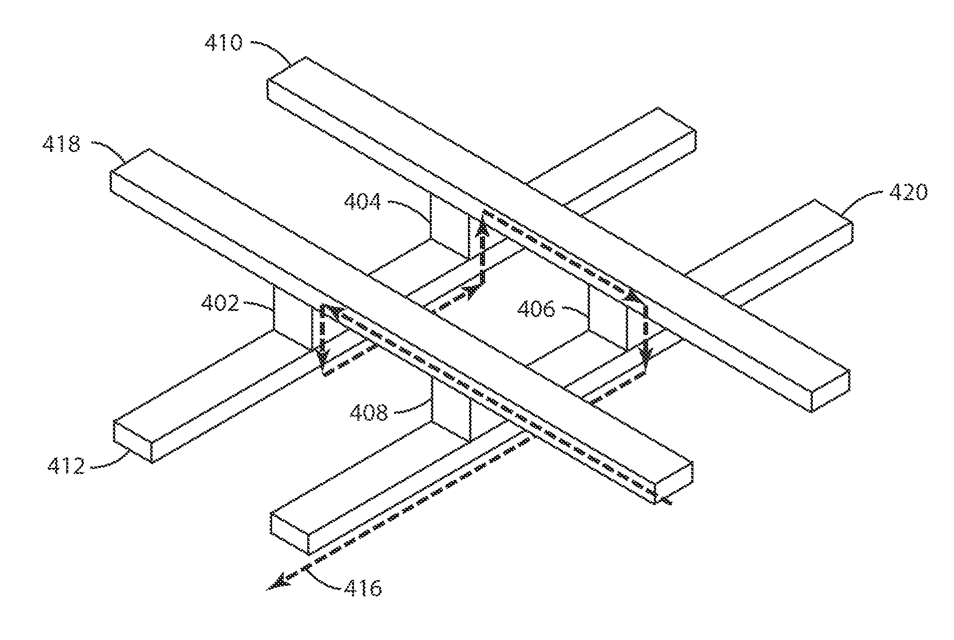
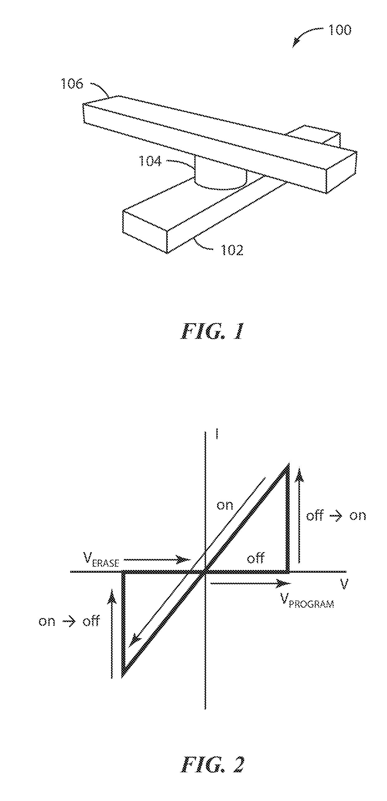
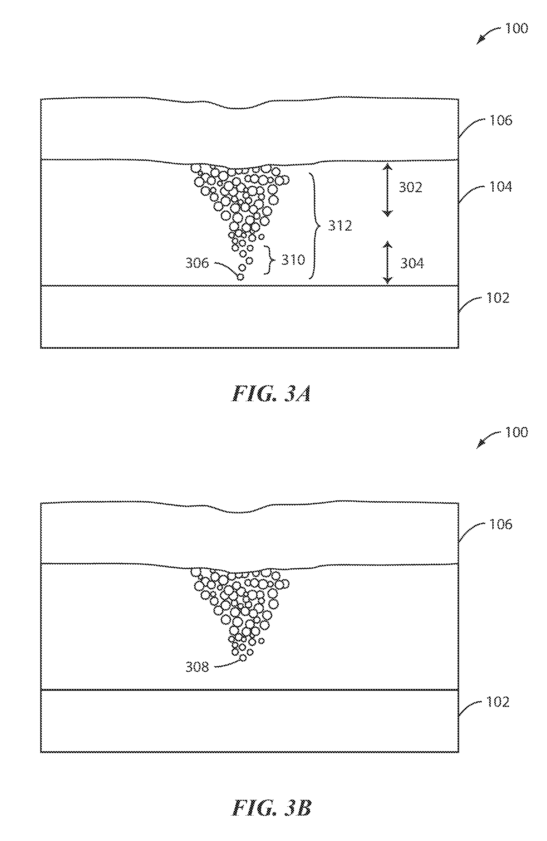
[0028]The present invention is generally directed to a memory device. More particularly, the present invention provides a structure and a method for a resistive switching cell having a nonlinear element. The switching cell may be used in a Resistive Random Access Memory (RRAM) or any highly integrated device. It should be recognized that embodiments of the present invention can have a broader range of applicability. Although the present invention is described with respect to specific embodiments, the embodiments are only used for illustrative purposes and should not be considered limiting.

[0029]RRAM is typically a two terminal device in which a switching element is sandwiched between a top electrode and a bottom electrode. The resistance of the switching element is varied by applying a voltage to the electrodes or a current through the switching element. Resistive switching can be bipolar or unipolar. In bipolar switching, the change in resistance of the switching element depends on...


PUM


Abstract

A switching device includes a substrate; a first electrode formed over the substrate; a second electrode formed over the first electrode; a switching medium disposed between the first and second electrode; and a nonlinear element disposed between the first and second electrodes and electrically coupled in series to the first electrode and the switching medium. The nonlinear element is configured to change from a first resistance state to a second resistance state on application of a voltage greater than a threshold.

Description

BACKGROUND[0001]The present invention is related to switching devices. More particularly, the present invention provides a structure and a method for forming non-volatile resistive switching memory devices characterized by a suppression of current at low bias and a high measured ON / OFF resistance ratio.[0002]The success of semiconductor devices has been mainly driven by an intensive transistor down-scaling process. However, as field effect transistors (FET) approach sizes less than 100 nm, problems such as short channel effect start to prevent proper device operation. Moreover, such sub 100 nm device size can lead to sub-threshold slope non-scaling and increased power dissipation. It is generally believed that transistor based memories such as those commonly known as Flash memory may approach an end to scaling within a decade. Flash memory is one type of non-volatile memory device.[0003]Other non-volatile random access memory (RAM) devices such as ferroelectric RAM (Fe RAM), magneto...

Claims


Application Information

Patent Timeline
IPC IPC(8): H01L47/00
CPCH01L27/101H01L45/085H01L27/2463H01L45/148H01L27/2409H01L45/1233H03M7/607H03M7/6088H03M7/6052H10B63/20H10B63/80H10N70/245H10N70/884H10N70/826H10B53/30
Inventor LU, WEIJO, SUNG HYUN
Owner CROSSBAR INC
Why Eureka
Try Eureka