Shared non-volatile storage for digital power control

a technology of digital power control and non-volatile storage, applied in the field of information handling systems, can solve the problems of adding to the total system bill of materials, outweighing the benefit of migrating most of the remaining power controller devices, etc., and achieves the flexibility of increasing nvram space, reducing the cost of nvram storage, and increasing the security of power system firmwar

Active Publication Date: 2012-12-20
DELL PROD LP
View PDF3 Cites 29 Cited by
  • Summary
  • Abstract
  • Description
  • Claims
  • Application Information

AI Technical Summary

Benefits of technology

[0007]Using the disclosed systems and methods, multiple power controller devices may arbitrate amongst themselves for ownership of shared NVRAM (e.g., a single common NVRAM device), and each power controller device may access only one or more sections of the shared NVRAM that are designated for that given power controller device. The disclosed systems and methods may also be implemented without a central agent current host (with BIOS SPI-Flash storing multiple option ROM images for several devices), but instead the multiple power controller devices are arbitrating amongst themselves for ownership of the shared NVRAM and accessing only certain sections of the shared NVRAM. In those embodiments where a single common NVRAM device is employed with multiple power controller devices, power system firmware security may be increased over the conventional multi-NVRAM distributed topology since only one NVRAM device is programmable with only one agent (e.g., a BMC) having write access. Moreover the customer image update process may be simplified by providing a consolidated update method for all digital power controllers, rather than using many discrete steps in the manner employed for conventional distributed NVRAM topologies. Additionally, the flexibility for increasing NVRAM space may be realized.
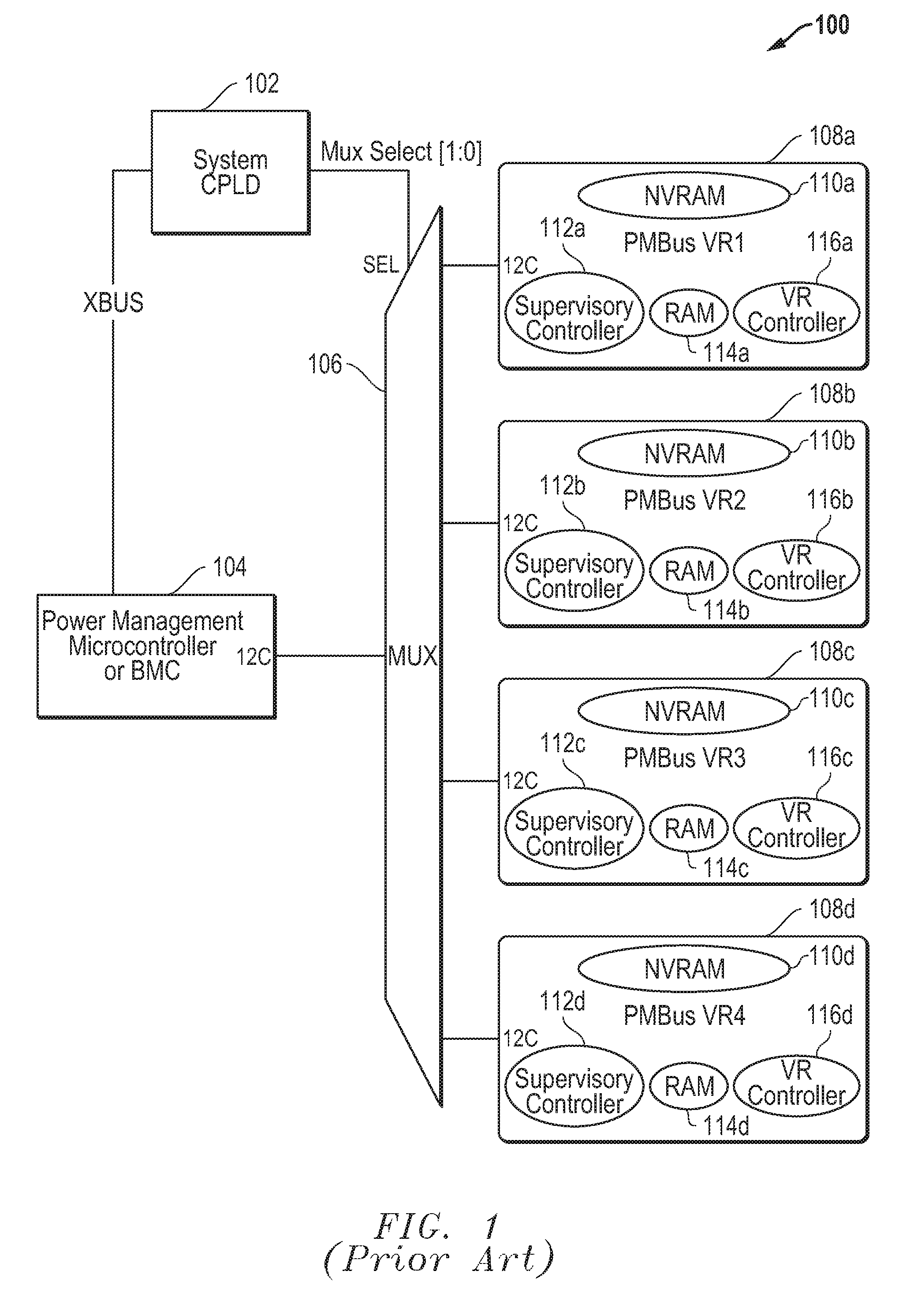
[0008]The disclosed systems and methods may be implemented to consolidate and reduce the number of NVRAM devices required for a given number of multiple power controller devices, and also do not require that NVRAM be integrated into each digital power controller device in the conventional manner. The disclosed systems and methods may therefore be implemented to improve and enhance advantages made possible with digital power controller devices by reducing the silicon area required to implement NVRAM with a digital power controller device, thus facilitating the transition from analog interfaces to digital interfaces for information handling system power controller devices such as voltage regulators. Because the cost for implementing individual NVRAM on each digital power controller device in the conventional manner substantially adds to the total system bill of material (e.g., a 50% cost adder to the total silicon cost budget), addition of digital power controller devices with integrated NVRAM in many circumstances outweighs the benefit of migrating most of the remaining power controller devices of an information handling system to a digital interface architecture. In contrast, the disclosed systems and methods may be implemented to provide a cost effective way to configure all or substantially all voltage regulators of an information handling system (such as a computer server) as digital power controller devices.
[0009]Thus, a consolidated NVRAM power device subsystem topology may be implemented in one embodiment to provide an information handling system with reduced printed circuit board (PCB) footprint space for various system boards since the total Flash Memory count is reduced. Additionally, better use of the power controller device silicon area may be enabled, e.g. providing the opportunity for bigger RAM on each power device (e.g., allowing better / longer averaging, temporary black-box, etc), or for other control logic. Moreover, lower cost may be provided for each digital power controller device of the system (e.g., to achieve about a 50% cost saving per power controller device), as well as a further cost reduction for a reduced number of NVRAM needed. This translates to lower overall system cost since the NVRAM are shared among the digital power controller devices, while at the same time making practical the proliferation of additional digital controller power devices on a computer server or other information handling system to support smart power management, i.e., facilitating the implementation of digital power controllers at higher adoption rates due to ease of use, lower cost, and reduced board footprints. Additionally, the manufacturing flow logistics and the ICT / PCBA test programming process may be simplified, leading to increased throughput.
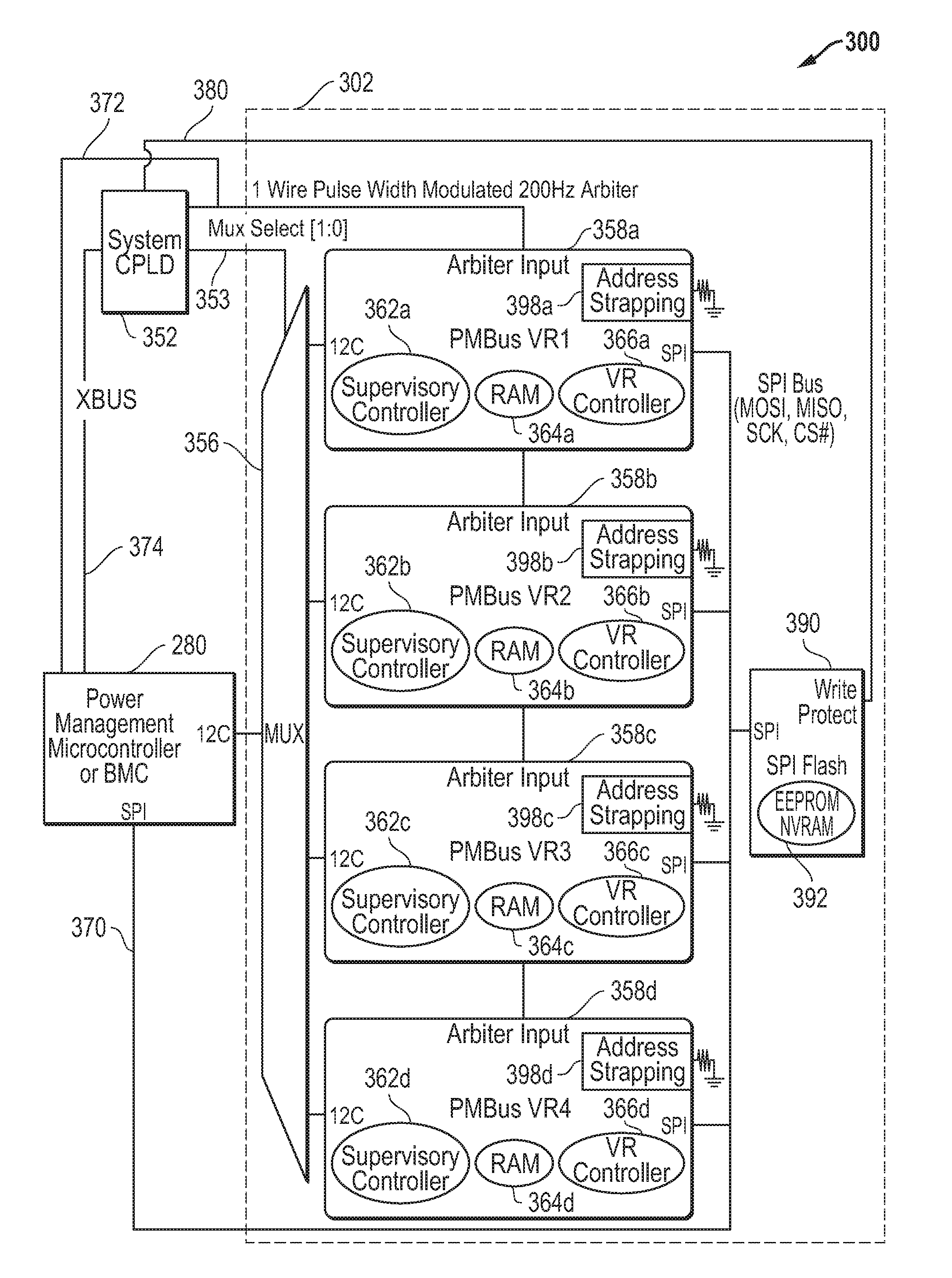
[0010]In one exemplary embodiment, an information handling system (e.g., such as a computer server) having multiple digital power controller devices may be implemented using a single commodity NVRAM device that is used for all digital power controller devices, thus reducing digital power controller cost. A shared serial peripheral interface (SPI) bus may be provided with multi master support (e.g., including each power controller device and a BMC or power management microcontroller or other suitable processing device) and single slave (e.g., a SPI Flash NVRAM). A pulse width modulated arbitration sequence or pattern may be implemented with a complex programmable logic device (CPLD) that drives a single-wire arbiter signal (i.e., that is duty-cycle based) and that provides direction for time-domain multiplexed SPI Flash owner to each digital power controller device as well as the Baseboard Management Controller. In this exemplary embodiment, each digital power controller device has read-only access to the single SPI Flash NVRAM, and is assigned a corresponding dedicated private address space (or offset) within the SPI Flash NVRAM with the private memory space for a given digital power controller device being determined within the SPI Flash by the address strapping of the corresponding given power controller device. Public address space may also be provided at the top address range (e.g., remaining space in SPI Flash NVRAM) for common storage (e.g., such as for System ID, etc.). As so implemented, increased security may be provided in one embodiment for the power firmware (i.e., having only one programmable NVRAM with only one agent having write access to the NVRAM). Further, the customer image update process may be simplified in one embodiment by providing a consolidated update method for all digital controllers vs. many discrete steps.

Problems solved by technology

Because the cost for implementing individual NVRAM on each digital power controller device in the conventional manner substantially adds to the total system bill of material (e.g., a 50% cost adder to the total silicon cost budget), addition of digital power controller devices with integrated NVRAM in many circumstances outweighs the benefit of migrating most of the remaining power controller devices of an information handling system to a digital interface architecture.

Method used


Image

  • Shared non-volatile storage for digital power control
  • Shared non-volatile storage for digital power control
  • Shared non-volatile storage for digital power control

Examples


Embodiment Construction

[0020]FIG. 2 is a block diagram of an information handling system 200 as it may be configured as a computer server system according to one exemplary embodiment of the disclosed systems. As shown in FIG. 2, information handling system 200 of this exemplary embodiment includes central processing units (CPUs) 205a and 205b, which may each be an Intel Pentium series processor, an Advanced Micro Devices (AMD) processor or one of many other processors currently available. System memory devices 215a and 215b are coupled as shown to CPUs 205a and 205b, respectively. An input output hub (IOH) 210 is coupled to each processor 205a and 205b, and an Intel controlled hub (ICH) chip 230 is coupled to IOH 210 to facilitate input / output functions for the information handling system. Also coupled to IOH 210 is local area network on motherboard (LOM) 238. Media drives (e.g., hard disk drives or other suitable media drive devices) 235 are coupled to ICH chip 230 to provide permanent storage for the in...


PUM


Abstract

Systems and methods may be implemented in a power device subsystem topology to provide an arbitration and communication scheme between a single consolidated non-volatile random access (NVRAM) memory device and multiple discrete digital power controller devices in a manner that provides data protection and the ability to update the full NVRAM content when needed.

Description

FIELD OF THE INVENTION[0001]This invention relates generally to information handling systems and, more particularly, to non-volatile storage for digital power control used with information handling systems.BACKGROUND OF THE INVENTION[0002]As the value and use of information continues to increase, individuals and businesses seek additional ways to process and store information. One option available to users is information handling systems. An information handling system generally processes, compiles, stores, and / or communicates information or data for business, personal, or other purposes thereby allowing users to take advantage of the value of the information. Because technology and information handling needs and requirements vary between different users or applications, information handling systems may also vary regarding what information is handled, how the information is handled, how much information is processed, stored, or communicated, and how quickly and efficiently the infor...

Claims


Application Information

Patent Timeline
Patent Type & Authority Applications(United States)
IPC IPC(8): G06F1/26
CPCG06F1/26
Inventor RAHARDJO, JOHANMATHEW, ABEY K.RICHARDS, III, GEORGE G.BREEN, JOHN J.LAMBERT, TIMOTHY M.
Owner DELL PROD LP
Why Eureka
Try Eureka